SBVS250 April   2015 TPS3779 , TPS3780

PRODUCTION DATA.  

  1. Features
  2. Applications
  3. Description
  4. Revision History
  5. Device Comparison Table
  6. Pin Configuration and Functions
  7. Specifications
    1. 7.1 Absolute Maximum Ratings
    2. 7.2 ESD Ratings
    3. 7.3 Recommended Operating Conditions
    4. 7.4 Thermal Information
    5. 7.5 Electrical Characteristics
    6. 7.6 Timing Requirements
    7. 7.7 Typical Characteristics
  8. Detailed Description
    1. 8.1 Overview
    2. 8.2 Functional Block Diagrams
    3. 8.3 Feature Description
      1. 8.3.1 Inputs (SENSE1, SENSE2)
      2. 8.3.2 Outputs (OUT1, OUT2)
    4. 8.4 Device Functional Modes
      1. 8.4.1 Normal Operation (VDD ≥ VDD(min))
      2. 8.4.2 Power-On Reset (VDD < V(POR))
  9. Application and Implementation
    1. 9.1 Application Information
      1. 9.1.1 Threshold Overdrive
      2. 9.1.2 Sense Resistor Divider
    2. 9.2 Typical Applications
    3. 9.3 Monitoring Two Separate Rails
      1. 9.3.1 Design Requirements
      2. 9.3.2 Detailed Design Procedure
      3. 9.3.3 Application Curve
    4. 9.4 Early Warning Detection
      1. 9.4.1 Design Requirements
      2. 9.4.2 Detailed Design Procedure
      3. 9.4.3 Application Curve
  10. 10Power-Supply Recommendations
  11. 11Layout
    1. 11.1 Layout Guidelines
    2. 11.2 Layout Example
  12. 12Device and Documentation Support
    1. 12.1 Device Support
      1. 12.1.1 Development Support
        1. 12.1.1.1 Evaluation Modules
        2. 12.1.1.2 Spice Models
      2. 12.1.2 Device Nomenclature
    2. 12.2 Documentation Support
      1. 12.2.1 Related Documentation
        1. 12.2.1.1 Related Documentation
    3. 12.3 Related Links
    4. 12.4 Trademarks
    5. 12.5 Electrostatic Discharge Caution
    6. 12.6 Glossary
  13. 13Mechanical, Packaging, and Orderable Information

Package Options

Mechanical Data (Package|Pins)
Thermal pad, mechanical data (Package|Pins)
Orderable Information

11 Layout

11.1 Layout Guidelines

Place the VDD decoupling capacitor close to the device.

Avoid using long traces for the VDD supply node. The VDD capacitor, along with parasitic inductance from the supply to the capacitor, can form an LC tank and create ringing with peak voltages above the maximum VDD voltage.

11.2 Layout Example
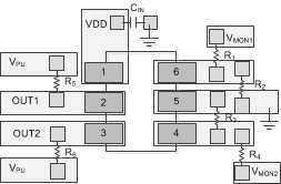
TPS3779 TPS3780 dbv_lay_sbvs250.gifFigure 26. Example SOT23 Layout