SBVS050M May   2004  – March 2023 TPS3808

PRODUCTION DATA  

  1. Features
  2. Applications
  3. Description
  4. Revision History
  5. Device Voltage Thresholds
  6. Pin Configuration and Functions
  7. Specifications
    1. 7.1 Absolute Maximum Ratings
    2. 7.2 ESD Ratings
    3. 7.3 Recommended Operating Conditions
    4. 7.4 Thermal Information
    5. 7.5 Electrical Characteristics
    6. 7.6 Switching Characteristics
    7. 7.7 Typical Characteristics
  8. Detailed Description
    1. 8.1 Overview
    2. 8.2 Functional Block Diagram
    3. 8.3 Feature Description
      1. 8.3.1 SENSE Input
      2. 8.3.2 Selecting the RESET Delay Time
      3. 8.3.3 Manual RESET ( MR) Input
      4. 8.3.4 RESET Output
    4. 8.4 Device Functional Modes
      1. 8.4.1 Normal Operation (VDD > VDD(min))
      2. 8.4.2 Above Power-On Reset but Less Than VDD(min) (VPOR < VDD < VDD(min))
      3. 8.4.3 Below Power-On Reset (VDD < VPOR)
  9. Application and Implementation
    1. 9.1 Application Information
    2. 9.2 Typical Application
      1. 9.2.1 Design Requirements
      2. 9.2.2 Detailed Design Procedure
        1. 9.2.2.1 Immunity to SENSE Pin Voltage Transients
      3. 9.2.3 Application Curve
  10. 10Power Supply Recommendations
  11. 11Layout
    1. 11.1 Layout Guidelines
    2. 11.2 Layout Example
  12. 12Device and Documentation Support
    1. 12.1 Device Support
      1. 12.1.1 Development Support
        1. 12.1.1.1 Evaluation Modules
    2. 12.2 Documentation Support
      1. 12.2.1 Related Documentation
    3. 12.3 Support Resources
    4. 12.4 Trademarks
    5. 12.5 Electrostatic Discharge Caution
    6. 12.6 Glossary
  13. 13Mechanical, Packaging, and Orderable Information

Package Options

Mechanical Data (Package|Pins)
Thermal pad, mechanical data (Package|Pins)
Orderable Information

Typical Characteristics

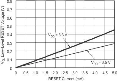
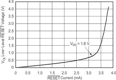
At TJ = 25°C, VDD = 3.3 V, RLRESET = 100 kΩ, and CLRESET = 50 pF, unless otherwise noted.

GUID-95D04BDE-A586-4FAB-A764-811C62BD0133-low.gif
Figure 7-2 Supply Current vs Supply Voltage
GUID-80D6632F-A8D6-4457-8B70-D81CA85DCB0C-low.gif
Figure 7-4 Normalized RESET Time-Out Period vs Temperature (CT = Open, CT = VDD, CT = Any)
GUID-AEFC6639-61B9-4CDD-A0BE-A47A05D69B44-low.gif
Figure 7-6 Normalized Sense Threshold Voltage (VIT) vs Temperature
GUID-30B9F946-7D35-45DB-A848-54632DA2726E-low.gif
Figure 7-8 Low-Level RESET Voltage vs RESET Current
GUID-D5682ED2-0A59-4563-A6F0-8EA9B145403E-low.gif
Figure 7-3 RESET Time-Out Period vs CT
GUID-0B82DAE2-79FC-4350-AF44-178933026A74-low.gif
Figure 7-5 Maximum Transient Duration at Sense vs Sense Threshold Overdrive Voltage
GUID-35AF8517-7777-41E0-9ECA-BFA511FA22FE-low.gif
Figure 7-7 Low-Level RESET Voltage vs RESET Current