SLVS228D August 1999 – December 2020
PRODUCTION DATA
- 1Features
- 2Applications
- 3Description
- 4Revision History
- 5Device Comparison
- 6Pin Configuration and Functions
- 7Specifications
- 8Detailed Description
- 9Electrostatic Discharge Caution
Package Options
Mechanical Data (Package|Pins)
- DBV|3
Thermal pad, mechanical data (Package|Pins)
Orderable Information
6 Pin Configuration and Functions
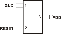
 Figure 6-1 Pin configuration
Table 6-1 Pin Functions
| PIN | I/O(1) | DESCRIPTION | |
|---|---|---|---|
| NAME | NO. | ||
| GND | 1 | - | This pin should be connected to ground with a low-impedance connection. |
| RESET | 2 | O | RESET is an active low
signal, asserting when VDD is below the threshold voltage. When
VDD rises above VIT, there is a delay time (td)
until RESET deasserts. RESET is a push-pull output stage. |
| VDD | 3 | - | Supply voltage pin. A 0.1-µF ceramic capacitor from this pin to ground is recommended to improve stability of the threshold voltage |