SLVS331J December   2000  – August 2024 TPS3813

PRODUCTION DATA  

  1.   1
  2. Features
  3. Applications
  4. Description
  5. Device Comparison Table
  6. Pin Configuration and Functions
  7. Specifications
    1. 6.1 Absolute Maximum Ratings
    2. 6.2 ESD Ratings
    3. 6.3 Recommended Operating Conditions
    4. 6.4 Thermal Information
    5. 6.5 Electrical Characteristics
    6. 6.6 Timing Requirements
    7. 6.7 Switching Characteristics
    8. 6.8 Dissipation Ratings
    9. 6.9 Typical Characteristics
  8. Detailed Description
    1. 7.1 Overview
    2. 7.2 Functional Block Diagram
    3. 7.3 Feature Description
      1. 7.3.1 Input Voltage (VDD)
        1. 7.3.1.1 VDD Hysteresis
        2. 7.3.1.2 VDD Glitch Immunity
      2. 7.3.2 User-Programmable Watchdog Timer (WDI)
      3. 7.3.3 RESET Output
    4. 7.4 Device Functional Modes
      1. 7.4.1 Normal Operation (VDD > VIT)
      2. 7.4.2 Above Power-On Reset But Less Than Threshold (VPOR < VDD < VIT)
      3. 7.4.3 Below Power-On Reset (VDD < VPOR)
    5. 7.5 Programming
      1. 7.5.1 Implementing Window-Watchdog Settings
      2. 7.5.2 Programmable Window-Watchdog by Using an External Capacitor
      3. 7.5.3 Lower Boundary Calculation
      4. 7.5.4 Watchdog Software Considerations
      5. 7.5.5 Power-Up Considerations
  9. Application and Implementation
    1. 8.1 Application Information
    2. 8.2 Typical Application
      1. 8.2.1 Design Requirements
      2. 8.2.2 Detailed Design Procedure
      3. 8.2.3 Application Curve
    3. 8.3 Power Supply Recommendations
    4. 8.4 Layout
      1. 8.4.1 Layout Guidelines
      2. 8.4.2 Layout Example
  10. Device and Documentation Support
    1. 9.1 Related Links
    2. 9.2 Receiving Notification of Documentation Updates
    3. 9.3 Support Resources
    4. 9.4 Trademarks
    5. 9.5 Electrostatic Discharge Caution
    6. 9.6 Glossary
  11. 10Revision History
  12. 11Mechanical, Packaging, and Orderable Information

Package Options

Mechanical Data (Package|Pins)
Thermal pad, mechanical data (Package|Pins)
Orderable Information

Pin Configuration and Functions

TPS3813 DBV
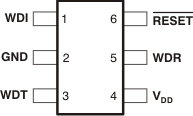
                        Package6-Pin SOT-23Top ViewFigure 5-1 DBV Package
6-Pin SOT-23
Top View
Table 5-1 Pin Functions
PIN I/O DESCRIPTION
NO. NAME
1 WDI I Watchdog timer input. This input must be driven at all times and not left floating.
2 GND I Ground
3 WDT I Programmable watchdog delay input
4 VDD I Supply voltage and supervising input
5 WDR I Selectable watchdog window ratio input. This input must be tied to VDD or GND and not left floating.
6 RESET O Open-drain reset output