SLVS331J December   2000  – August 2024 TPS3813

PRODUCTION DATA  

  1.   1
  2. Features
  3. Applications
  4. Description
  5. Device Comparison Table
  6. Pin Configuration and Functions
  7. Specifications
    1. 6.1 Absolute Maximum Ratings
    2. 6.2 ESD Ratings
    3. 6.3 Recommended Operating Conditions
    4. 6.4 Thermal Information
    5. 6.5 Electrical Characteristics
    6. 6.6 Timing Requirements
    7. 6.7 Switching Characteristics
    8. 6.8 Dissipation Ratings
    9. 6.9 Typical Characteristics
  8. Detailed Description
    1. 7.1 Overview
    2. 7.2 Functional Block Diagram
    3. 7.3 Feature Description
      1. 7.3.1 Input Voltage (VDD)
        1. 7.3.1.1 VDD Hysteresis
        2. 7.3.1.2 VDD Glitch Immunity
      2. 7.3.2 User-Programmable Watchdog Timer (WDI)
      3. 7.3.3 RESET Output
    4. 7.4 Device Functional Modes
      1. 7.4.1 Normal Operation (VDD > VIT)
      2. 7.4.2 Above Power-On Reset But Less Than Threshold (VPOR < VDD < VIT)
      3. 7.4.3 Below Power-On Reset (VDD < VPOR)
    5. 7.5 Programming
      1. 7.5.1 Implementing Window-Watchdog Settings
      2. 7.5.2 Programmable Window-Watchdog by Using an External Capacitor
      3. 7.5.3 Lower Boundary Calculation
      4. 7.5.4 Watchdog Software Considerations
      5. 7.5.5 Power-Up Considerations
  9. Application and Implementation
    1. 8.1 Application Information
    2. 8.2 Typical Application
      1. 8.2.1 Design Requirements
      2. 8.2.2 Detailed Design Procedure
      3. 8.2.3 Application Curve
    3. 8.3 Power Supply Recommendations
    4. 8.4 Layout
      1. 8.4.1 Layout Guidelines
      2. 8.4.2 Layout Example
  10. Device and Documentation Support
    1. 9.1 Related Links
    2. 9.2 Receiving Notification of Documentation Updates
    3. 9.3 Support Resources
    4. 9.4 Trademarks
    5. 9.5 Electrostatic Discharge Caution
    6. 9.6 Glossary
  11. 10Revision History
  12. 11Mechanical, Packaging, and Orderable Information

Package Options

Mechanical Data (Package|Pins)
Thermal pad, mechanical data (Package|Pins)
Orderable Information

VDD Glitch Immunity

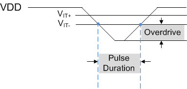
These devices are immune to quick voltage transient or excursion on VDD. Sensitivity to transients depends on both pulse duration (tGI_VIT) found in Section 6.6 and transient overdrive. Overdrive is defined by how much VDD exceeds the specified threshold. Threshold overdrive is calculated as a percent of the threshold in question, as shown in Equation 1.

Equation 1. Overdrive = | ((VDD / VIT) – 1) × 100% |

where

  • VIT = VIT- is the threshold voltage
  • VIT+ = VIT + VHYS is the rising threshold voltage
  • VDD is the input voltage crossing VIT
TPS3813 Overdrive Versus Pulse DurationFigure 7-1 Overdrive Versus Pulse Duration

TPS3813xxx devices have built-in glitch immunity (tGI_VIT) as shown in Section 6.6. Figure 7-1 shows that VDD must fall below VIT for tGI_VIT, otherwise the faling transistion is ignored. When VDD falls below VIT for tGI_VIT, RESET transitions low to indicate a fault condition after the propagation delay high-to-low (tPHL). When VDD rises above VIT+ = VIT + VHYS, RESET deasserts to a logic high indicating there is no more fault condition only if VDD remains above VIT+ for longer than the reset delay (tD).