SBVS193D June 2012 – July 2015 TPS3831 , TPS3839
PRODUCTION DATA.
- 1 Features
- 2 Applications
- 3 Description
- 4 Revision History
- 5 Device Options
- 6 Pin Configuration and Functions
- 7 Specifications
- 8 Detailed Description
- 9 Applications and Implementation
- 10Power Supply Recommendations
- 11Layout
- 12Device and Documentation Support
- 13Mechanical, Packaging, and Orderable Information
Package Options
Mechanical Data (Package|Pins)
Thermal pad, mechanical data (Package|Pins)
- DQN|4
Orderable Information
8 Detailed Description
8.1 Overview
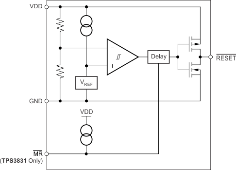
The TPS3831 and TPS3839 are ultralow current voltage supervisory circuits that monitor the input supply voltage of these devices. Both devices assert an active-low reset whenever the VDD supply voltage drops below the negative-going threshold voltage (VIT–). The output, RESET, remains asserted for approximately
200 ms after the VDD voltage rises above the positive-going threshold voltage (VIT– + Vhys). These devices are designed to ignore fast transients on the VDD pin.
The TPS3831 device includes a manual reset input (MR) that can be used to force the RESET signal low, even if the supply voltage is above VIT–.
8.3 Feature Description
8.3.1 VDD Transient Rejection
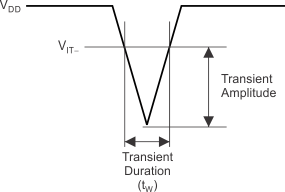
The TPS383x (TPS3831 and TPS3839) devices have built-in rejection of fast transients on the VDD pin. Transient rejection depends on both the duration and amplitude of the transient. Transient amplitude is measured from the bottom of the transient to the negative threshold voltage (VIT–) of the device, as shown in Figure 12.
 Figure 12. Voltage Transient Measurement
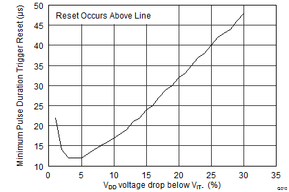
Figure 13 shows the relationship between the transient amplitude and duration required to trigger a reset. Any combination of duration and amplitude greater than that shown in Figure 13 generates a reset signal.
 Figure 13. TPS3839 Transient Rejection
8.3.2 Manual Reset (MR) Input (TPS3831 Only)
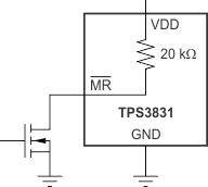
The manual reset (MR) input allows a processor, or other logic devices, to initiate a reset (TPS3831 device only). A logic low (0.3 VDD) on MR causes RESET to assert. After MR returns to a logic high and VDD is greater than the threshold voltage, RESET is deasserted after the reset delay time, td, elapses. MR is internally tied to VDD with a 20-kΩ resistor; therefore, this pin can be left unconnected if MR is not used. If a logic signal driving MR does not go fully to VDD, some additional current draws into VDD as a result of the internal pullup resistor on MR. To minimize current draw, a logic-level FET can be used, as shown in Figure 14.
 Figure 14. Using a Logic-Level FET to Minimize Current Draw
8.4 Device Functional Modes
8.4.1 Normal Operation (VDD > VDD(min))
When the voltage on VDD is greater than VDD(min), the RESET output corresponds to the voltage on the VDD pin relative to VIT–.
8.4.2 Below VDD(min) (V(POR) < VDD < VDD(min)
When the voltage on VDD is less than VDD(min) but greater than the power-on reset voltage (V(POR)), the RESET output is asserted.
8.4.3 Below Power-On Reset (VDD < V(POR)
When the voltage on VDD is lower than the power-on reset voltage (V(POR)), the RESET output is undefined. Do not rely on the RESET output for proper device function under this condition.
