SNVSBA1B April 2019 – April 2020 TPS3840-Q1
PRODUCTION DATA.
- 1 Features
- 2 Applications
- 3 Description
- 4 Revision History
- 5 Device Comparison
- 6 Pin Configuration and Functions
- 7 Specifications
- 8 Detailed Description
- 9 Application and Implementation
- 10Power Supply Recommendations
- 11Layout
- 12Device and Documentation Support
- 13Mechanical, Packaging, and Orderable Information
Package Options
Mechanical Data (Package|Pins)
- DBV|5
Thermal pad, mechanical data (Package|Pins)
Orderable Information
6 Pin Configuration and Functions
DBV Package
5-Pin
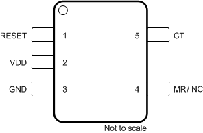
TPS3840PL-Q1, TPS3840DL-Q1 Top View
 Figure 2. Pin Configuration TPS3840PL-Q1, TPS3840DL-Q1
 DBV Package
5-Pin
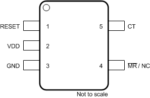
TPS3840PH-Q1 Top View
 Figure 3. Pin Configuration TPS3840PH-Q1
 Pin Functions
| PIN | I/O | DESCRIPTION | ||
|---|---|---|---|---|
| NAME | TPS3840PL-Q1, TPS3840DL-Q1 | TPS3840PH-Q1 | ||
| RESET | N/A | 1 | O | Active-High Output Reset Signal: This pin is driven high when either the MR pin is driven to a logic low or VDD voltage falls below the negative voltage threshold (VIT-). RESET remains high (asserted) for the delay time period (tD) after both MR is floating or above VMR_L and VDD voltage rise above VIT+. |
| RESET | 1 | N/A | O | Active-Low Output Reset Signal: This pin is driven logic when either the MR pin is driven to a logic low or VDD voltage falls below the negative voltage threshold (VIT-). RESET remains low (asserted) for the delay time period (tD) after both MR is floating or above VMR_L and VDD voltage rise above VIT+. |
| VDD | 2 | 2 | I | Input Supply Voltage. TPS3840-Q1 monitors VDD voltage |
| GND | 3 | 3 | _ | Ground |
| MR / NC | 4 | 4 | I | Manual Reset. Pull this pin to a logic low (VMR_L) to assert a reset signal in the output pin. After the MR pin is left floating or pull to VMR_H the output goes to the nominal state after the reset delay time(tD) expires. MR can be left floating when not in use. NC stands for "No Connection" or floating. |
| CT | 5 | 5 | - | Capacitor Time Delay Pin. The CT pin offers a user-programmable delay time. Connect an external capacitor on this pin to adjust time delay. When not in use leave pin floating for the smallest fixed time delay. |