SNVSBA1B April 2019 – April 2020 TPS3840-Q1
PRODUCTION DATA.
- 1 Features
- 2 Applications
- 3 Description
- 4 Revision History
- 5 Device Comparison
- 6 Pin Configuration and Functions
- 7 Specifications
- 8 Detailed Description
- 9 Application and Implementation
- 10Power Supply Recommendations
- 11Layout
- 12Device and Documentation Support
- 13Mechanical, Packaging, and Orderable Information
Package Options
Mechanical Data (Package|Pins)
- DBV|5
Thermal pad, mechanical data (Package|Pins)
Orderable Information
7.6 Timing Requirements
At 1.5 V ≤ VDD ≤ 10 V, CT = MR = Open, RESET pull-up resistor (Rpull-up) = 100 kΩ to VDD, output reset load (CLOAD) = 10 pF and over the operating free-air temperature range – 40°C to 125°C, VDD slew rate < 100mV / us, unless otherwise noted. Typical values are at TJ = 25°C.| PARAMETER | TEST CONDITIONS | MIN | TYP | MAX | UNIT | |
|---|---|---|---|---|---|---|
| tSTRT | Startup Delay(1) | CT pin open | 100 | 220 | 350 | µs |
| tP_HL | Propagation detect delay for VDD falling below VIT- | VDD = VIT+ to (VIT-) - 10%(2) | 15 | 30 | µs | |
| tD | Reset time delay(3) | CT pin = open
|
50 | µs | ||
| CT pin = 10 nF | 6.2 | ms | ||||
| CT pin = 1 µF | 619 | ms | ||||
| tGI_VIT- | Glitch immunity VIT- | 5% VIT- overdrive(4) | 10 | µs | ||
| tMR_PW | MR pin pulse duration to initiate reset | 300 | ns | |||
| tMR_RES | Propagation delay from MR low to reset | VDD = 4.5 V, MR < VMR_L | 700 | ns | ||
| tMR_tD | Delay from release MR to deasert reset | VDD = 4.5 V,
MR = VMR_L to VMR_H |
tD | ms | ||

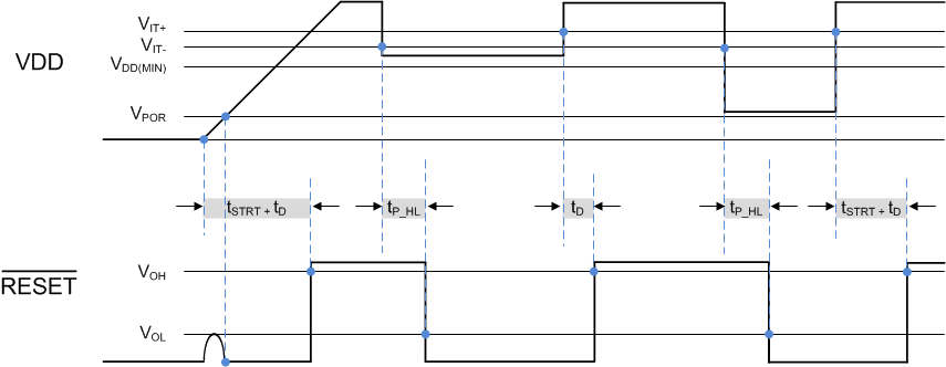
1. tD (no cap) is included in tSTRT time delay. If tD delay is programmed by an external capacitor connected to CT pin then tD programmed time will be added to the startup time, VDD slew rate = 100 mV / µs.
2. Open-Drain timing diagram assumes pull-up resistor is connected to RESET
Figure 4. Timing Diagram TPS3840DL-Q1 (Open-Drain Active-Low) 
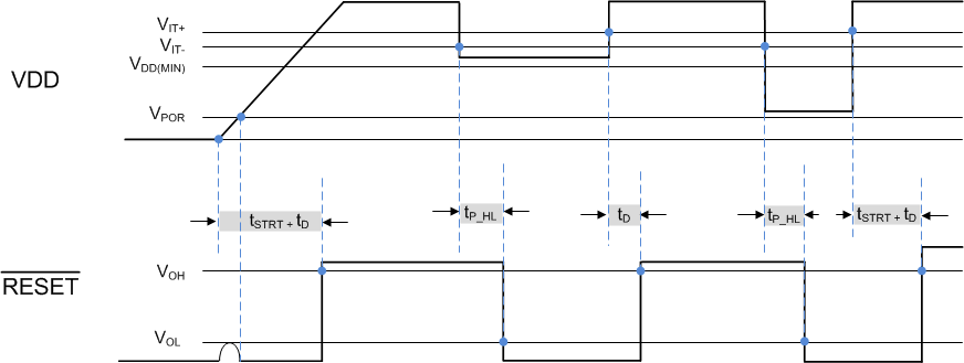
1. tD (no cap) is included in tSTRT time delay. If tD delay is programmed by an external capacitor connected to CT pin, then tD programmed time will be added to the startup time. VDD slew rate = 100 mV / µs.
Figure 5. Timing Diagram TPS3840PL-Q1 (Push-Pull Active-Low) 
1. tD (no cap) is included in tSTRT time delay. If tD delay is programmed by an external capacitor connected to CT pin, then tD programmed time will be added to the total startup time. VDD slew rate = 100 mV / µs.
Figure 6. Timing Diagram TPS3840PH-Q1 (Push-Pull Active-High)