SNVSB03D December   2018  – January 2020 TPS3840

PRODUCTION DATA.  

  1. Features
  2. Applications
  3. Description
    1.     Device Images
      1.      Typical Application Circuit
      2.      TPS3840 Typical Supply Current
  4. Revision History
  5. Device Comparison
  6. Pin Configuration and Functions
    1.     Pin Functions
  7. Specifications
    1. 7.1 Absolute Maximum Ratings
    2. 7.2 ESD Ratings
    3. 7.3 Recommended Operating Conditions
    4. 7.4 Thermal Information
    5. 7.5 Electrical Characteristics
    6. 7.6 Timing Requirements
    7. 7.7 Typical Characteristics
  8. Detailed Description
    1. 8.1 Overview
    2. 8.2 Functional Block Diagram
    3. 8.3 Feature Description
      1. 8.3.1 Input Voltage (VDD)
        1. 8.3.1.1 VDD Hysteresis
        2. 8.3.1.2 VDD Transient Immunity
      2. 8.3.2 User-Programmable Reset Time Delay
      3. 8.3.3 Manual Reset (MR) Input
      4. 8.3.4 Output Logic
        1. 8.3.4.1 RESET Output, Active-Low
        2. 8.3.4.2 RESET Output, Active-High
    4. 8.4 Device Functional Modes
      1. 8.4.1 Normal Operation (VDD > VDD(min))
      2. 8.4.2 VDD Between VPOR and VDD(min)
      3. 8.4.3 Below Power-On-Reset (VDD < VPOR)
  9. Application and Implementation
    1. 9.1 Application Information
    2. 9.2 Typical Application
      1. 9.2.1 Design 1: Dual Rail Monitoring with Power-Up Sequencing
        1. 9.2.1.1 Design Requirements
        2. 9.2.1.2 Detailed Design Procedure
        3. 9.2.1.3 Application Curves
      2. 9.2.2 Design 2: Battery Voltage and Temperature Monitor
        1. 9.2.2.1 Design Requirements
        2. 9.2.2.2 Detailed Design Procedure
      3. 9.2.3 Design 3: Fast Start Undervoltage Supervisor with Level-shifted Input
        1. 9.2.3.1 Design Requirements
        2. 9.2.3.2 Detailed Design Procedure
      4. 9.2.4 Design 4: Voltage Monitor with Back-up Battery Switchover
        1. 9.2.4.1 Design Requirements
        2. 9.2.4.2 Detailed Design Procedure
      5. 9.2.5 Application Curve: TPS3840EVM
  10. 10Power Supply Recommendations
  11. 11Layout
    1. 11.1 Layout Guidelines
    2. 11.2 Layout Example
  12. 12Device and Documentation Support
    1. 12.1 Device Nomenclature
    2. 12.2 Support Resources
    3. 12.3 Trademarks
    4. 12.4 Electrostatic Discharge Caution
    5. 12.5 Glossary
  13. 13Mechanical, Packaging, and Orderable Information

Package Options

Mechanical Data (Package|Pins)
Thermal pad, mechanical data (Package|Pins)
Orderable Information

Design 4: Voltage Monitor with Back-up Battery Switchover

A typical application for the TPS3840 is to monitor a voltage rail and switch the power to a back-up battery if the main supply is in undervoltage condition. Because systems that utilize a back-up battery tend to require low quiescent current, TPS3840 serves as the perfect solution as this device only requires 350 nA typically. The TPS3840 monitors the main power rail via the VDD pin and when the main power rail falls, the RESET output asserts causing a switch to close on the back-up battery rail. The diodes provide an ORing logic function to prevent reverse leakage and to allow either rail to connect to the output depending on the status of the main voltage rail.
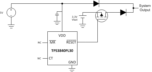
TPS3840 Typical_Application_4rev4.gifFigure 53. Voltage Monitor with Back-up Battery Switchover Solution