SBVS285 February 2017 TPS3852-Q1
PRODUCTION DATA.
- 1 Features
- 2 Applications
- 3 Description
- 4 Revision History
- 5 Pin Configuration and Functions
- 6 Specifications
- 7 Detailed Description
- 8 Application and Implementation
- 9 Power Supply Recommendations
- 10Layout
- 11Device and Documentation Support
- 12Mechanical, Packaging, and Orderable Information
Package Options
Refer to the PDF data sheet for device specific package drawings
Mechanical Data (Package|Pins)
- DRB|8
Thermal pad, mechanical data (Package|Pins)
- DRB|8
Orderable Information
6.6 Timing Requirements
at VITN + VHYST ≤ VDD ≤ 6.5 V over the operating temperature range of –40°C ≤ TA, T J ≤ +125°C (unless otherwise noted); the open-drain pullup resistors are 10 kΩ for each output; typical values are at TJ = 25°C| MIN | TYP | MAX | UNIT | |||
|---|---|---|---|---|---|---|
| GENERAL | ||||||
| tINIT | CWD pin evaluation period | 381 | µs | |||
| Minimum MR, SET1 pin pulse duration | 1 | µs | ||||
| Startup delay | 300 | µs | ||||
| RESET FUNCTION | ||||||
| tRST | Reset timeout period | 170 | 200 | 230 | ms | |
| tRST-DEL | VDD to RESET delay | VDD = VITN + VHYST + 2.5% | 35 | µs | ||
| VDD = VITN – 2.5% | 17 | |||||
| tMR-DEL | MR to RESET delay | 200 | ns | |||
| Watchdog Function | ||||||
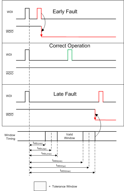
| tWDL | Window watchdog lower boundary | CWD = NC, SET1 = 0(1) | Watchdog disabled | |||
| CWD = NC, SET1 = 1(1) | 680 | 800 | 920 | ms | ||
| CWD = 10 kΩ to VDD, SET1 = 0(1) |
Watchdog disabled | |||||
| CWD = 10 kΩ to VDD, SET1 = 1(1) |
1.48 | 1.85 | 2.22 | ms | ||
| tWDU | Window watchdog upper boundary | CWD = NC, SET1 = 0(1) | Watchdog disabled | |||
| CWD = NC, SET1 = 1(1) | 1360 | 1600 | 1840 | ms | ||
| CWD = 10 kΩ to VDD, SET1 = 0(1) |
Watchdog disabled | |||||
| CWD = 10 kΩ to VDD, SET1 = 1(1) |
9.35 | 11.0 | 12.65 | ms | ||
| tWD-setup | Setup time required for device to respond to changes on WDI after being enabled | 150 | µs | |||
| Minimum WDI pulse duration | 50 | ns | ||||
| tWD-DEL | WDI to WDO delay | 50 | ns | |||
(1) SET1 = 0 means VSET1 < VIL, SET1 = 1 means VSET1 > VIH.
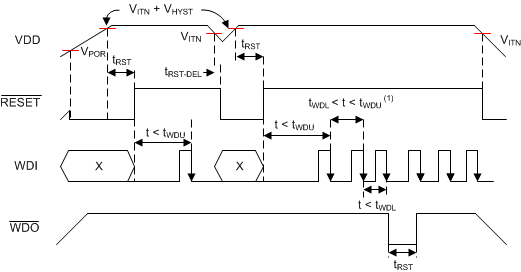
 Figure 2. TPS3852-Q1 Window Watchdog Timing