SBVS285 February   2017 TPS3852-Q1

PRODUCTION DATA.  

  1. Features
  2. Applications
  3. Description
    1.     Device Images
      1.      Typical Application Circuit
      2.      Undervoltage Threshold (VITN) Accuracy vs Temperature
  4. Revision History
  5. Pin Configuration and Functions
    1.     Pin Functions
  6. Specifications
    1. 6.1 Absolute Maximum Ratings
    2. 6.2 ESD Ratings
    3. 6.3 Recommended Operating Conditions
    4. 6.4 Thermal Information
    5. 6.5 Electrical Characteristics
    6. 6.6 Timing Requirements
    7. 6.7 Typical Characteristics
  7. Detailed Description
    1. 7.1 Overview
    2. 7.2 Functional Block Diagram
    3. 7.3 Feature Description
      1. 7.3.1 RESET
      2. 7.3.2 Manual Reset (MR)
      3. 7.3.3 Undervoltage Fault Detection
      4. 7.3.4 Watchdog Mode
        1. 7.3.4.1 SET1
        2. 7.3.4.2 Window Watchdog Timer
        3. 7.3.4.3 Watchdog Input (WDI)
        4. 7.3.4.4 CWD
        5. 7.3.4.5 Watchdog Output (WDO)
    4. 7.4 Device Functional Modes
      1. 7.4.1 VDD is Below VPOR (VDD < VPOR)
      2. 7.4.2 Above Power-On-Reset, But Less Than VDD(min) (VPOR ≤ VDD < VDD(min))
      3. 7.4.3 Normal Operation (VDD ≥ VDD(min))
  8. Application and Implementation
    1. 8.1 Application Information
      1. 8.1.1 CWD Functionality
        1. 8.1.1.1 Factory-Programmed Timing Options
        2. 8.1.1.2 Adjustable Capacitor Timing
      2. 8.1.2 Overdrive Voltage
    2. 8.2 Typical Application
      1. 8.2.1 Design Requirements
      2. 8.2.2 Detailed Design Procedure
        1. 8.2.2.1 Monitoring the 3.3-V Rail
        2. 8.2.2.2 Calculating RESET and the WDO Pullup Resistor
        3. 8.2.2.3 Setting the Window Watchdog
        4. 8.2.2.4 Watchdog Disabled During Initialization Period
      3. 8.2.3 Glitch Immunity
      4. 8.2.4 Application Curves
  9. Power Supply Recommendations
  10. 10Layout
    1. 10.1 Layout Guidelines
    2. 10.2 Layout Example
  11. 11Device and Documentation Support
    1. 11.1 Device Support
      1. 11.1.1 Development Support
        1. 11.1.1.1 Evaluation Module
      2. 11.1.2 Device Nomenclature
    2. 11.2 Receiving Notification of Documentation Updates
    3. 11.3 Community Resources
    4. 11.4 Trademarks
    5. 11.5 Electrostatic Discharge Caution
    6. 11.6 Glossary
  12. 12Mechanical, Packaging, and Orderable Information

Package Options

Refer to the PDF data sheet for device specific package drawings

Mechanical Data (Package|Pins)
  • DRB|8
Thermal pad, mechanical data (Package|Pins)
Orderable Information

Typical Characteristics

all curves are taken at 25°C with 1.6 V ≤ VDD ≤ 6.5 V (unless otherwise noted)
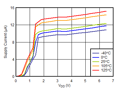
TPS3852-Q1 SupplyCurrentVsVDD.gif
Figure 3. Supply Current vs VDD
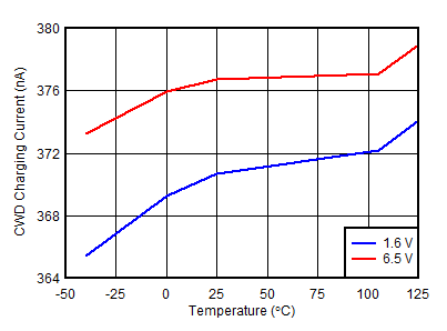
TPS3852-Q1 tc_CWD_Current_Vs_temp_SBVS301-01.gif
Figure 5. CWD Charging Current vs Temperature
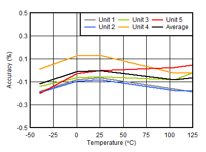
TPS3852-Q1 tc_vitn_acc_vs_temp_3_3.gif
TPS3852G33-Q1
Figure 7. VITN Accuracy vs Temperature
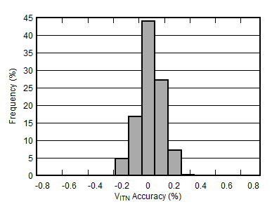
TPS3852-Q1 tc_vitn_acc_histogram.gif
Includes G and H versions with 3.3-V nominal monitored voltage,
total units = 15,536
Figure 9. VITN Accuracy Histogram
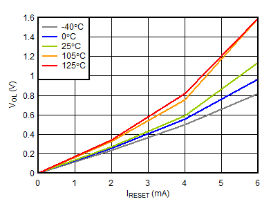
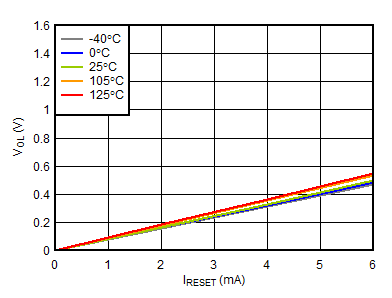
TPS3852-Q1 Vol_vs_Irst_1_6V_SBVS301-08.gif
VDD = 1.6 V
Figure 11. Low-Level RESET Voltage vs RESET Current
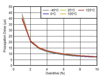
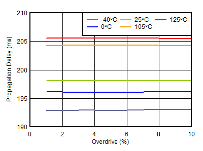
TPS3852-Q1 tc_propdelay_vs_overdrive_3.3V_enter_uv.gif
TPS3852G33-Q1 entering undervoltage
Figure 13. Propagation Delay vs Overdrive
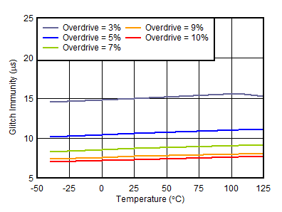
TPS3852-Q1 tc_glitchimmunity_3_3V.gif
VITN = 3.168 V
Figure 15. High-to-Low Glitch Immunity vs Temperature
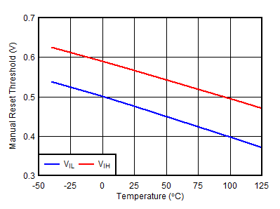
TPS3852-Q1 MR_threshold_vs_temp.gif
VDD = 1.6 V
Figure 4. MR Threshold vs Temperature
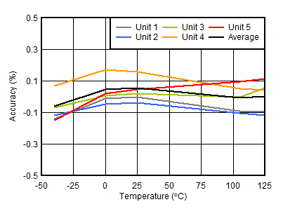
TPS3852-Q1 tc_vitn_vhyst_acc_vs_temp_3_3.gif
TPS3852G33-Q1
Figure 6. VITN + VHYST Accuracy vs Temperature
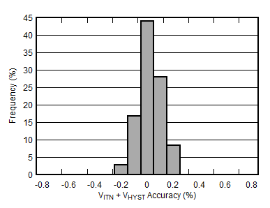
TPS3852-Q1 tc_vitn_vhyst_histogram.gif
Includes G and H versions with 3.3-V nominal monitored voltage,
total units = 15,536
Figure 8. VITN + VHYST Accuracy Histogram
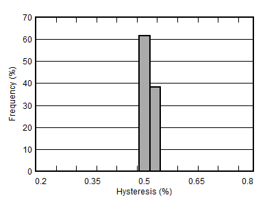
TPS3852-Q1 hysteresis_histogram.gif
Includes G and H versions with 3.3-V nominal monitored voltage,
total units = 15,536
Figure 10. Hysteresis Histogram
TPS3852-Q1 Vol_vs_Irst_6_5V_SBVS301-02.gif
VDD = 6.5 V
Figure 12. Low-Level RESET Voltage vs RESET Current
TPS3852-Q1 tc_propdelay_vs_overdrive_5V_exit_uv.gif
TPS3852G33-Q1 exiting undervoltage
Figure 14. Propagation Delay (tRST) vs Overdrive