SLVSA75A July 2010 – August 2015 TPS386596
PRODUCTION DATA.
- 1 Features
- 2 Applications
- 3 Description
- 4 Revision History
- 5 Pin Configuration and Functions
- 6 Specifications
- 7 Parameter Measurement Information
- 8 Detailed Description
- 9 Application and Implementation
- 10Power Supply Recommendations
- 11Layout
- 12Device and Documentation Support
- 13Mechanical, Packaging, and Orderable Information
Package Options
Mechanical Data (Package|Pins)
- DGK|8
Thermal pad, mechanical data (Package|Pins)
Orderable Information
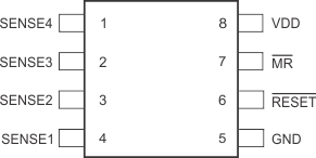
5 Pin Configuration and Functions
Pin Functions
| PIN | I/O | DESCRIPTION | ||
|---|---|---|---|---|
| NAME | NO. | |||
| GND | 5 | — | Ground | |
| MR | 7 | I | Manual reset input with internal 100-kΩ pullup to VDD and 50-ns deglitch. Logic low level of this pin asserts RESET. | |
| RESET | 6 | O | RESET is an open-drain output pin. When RESET is asserted, this pin remains in a low-impedance state. When RESET is deasserted, this pin goes to a high-impedance state after 50 ms. A pullup resistor to VDD or another voltage source is required. | |
| SENSE1 | 4 | I | Monitor voltage input for Supply 1 | When the voltage at this terminal drops the threshold voltage (VIT1= 2.9 V), RESET is asserted. |
| SENSE2 | 3 | I | Monitor voltage input for Supply 2 | When the voltage at this terminal drops the threshold voltage (VIT2= 0.4 V), RESET is asserted. |
| SENSE3 | 2 | I | Monitor voltage input for Supply 3 | When the voltage at this terminal drops the threshold voltage (VIT3= 0.4 V), RESET is asserted. |
| SENSE4 | 1 | I | Monitor voltage input for Supply 4 | When the voltage at this terminal drops the threshold voltage (VIT4= 0.4 V), RESET is asserted. |
| VDD | 8 | I | Supply voltage. Connecting a 0.1-µF ceramic capacitor close to this pin is recommended. | |
