SBVS303B March   2017  – February 2018 TPS3890-Q1

PRODUCTION DATA.  

  1. Features
  2. Applications
  3. Description
    1.     Device Images
      1.      Typical Application Circuit
      2.      VITN Accuracy vs Temperature
  4. Revision History
  5. Device Comparison Table
  6. Pin Configuration and Functions
    1.     Pin Functions
  7. Specifications
    1. 7.1 Absolute Maximum Ratings
    2. 7.2 ESD Ratings
    3. 7.3 Recommended Operating Conditions
    4. 7.4 Thermal Information
    5. 7.5 Electrical Characteristics
    6. 7.6 Timing Requirements
    7. 7.7 Typical Characteristics
  8. Detailed Description
    1. 8.1 Overview
    2. 8.2 Functional Block Diagram
    3. 8.3 Feature Description
      1. 8.3.1 User-Configurable RESET Delay Time
      2. 8.3.2 Manual Reset (MR) Input
      3. 8.3.3 RESET Output
      4. 8.3.4 SENSE Input
        1. 8.3.4.1 Immunity to SENSE Pin Voltage Transients
    4. 8.4 Device Functional Modes
      1. 8.4.1 Normal Operation (VDD > VDD(min))
      2. 8.4.2 Above Power-On-Reset But Less Than VDD(min) (VPOR < VDD < VDD(min))
      3. 8.4.3 Below Power-On-Reset (VDD < VPOR)
  9. Application and Implementation
    1. 9.1 Application Information
    2. 9.2 Typical Application
      1. 9.2.1 Design Requirements
      2. 9.2.2 Detailed Design Procedure
      3. 9.2.3 Application Curve
  10. 10Power Supply Recommendations
  11. 11Layout
    1. 11.1 Layout Guidelines
    2. 11.2 Layout Example
  12. 12Device and Documentation Support
    1. 12.1 Device Support
      1. 12.1.1 Device Nomenclature
    2. 12.2 Documentation Support
      1. 12.2.1 Related Documentation
    3. 12.3 Receiving Notification of Documentation Updates
    4. 12.4 Community Resources
    5. 12.5 Trademarks
    6. 12.6 Electrostatic Discharge Caution
    7. 12.7 Glossary
  13. 13Mechanical, Packaging, and Orderable Information

Package Options

Mechanical Data (Package|Pins)
Thermal pad, mechanical data (Package|Pins)
Orderable Information

Manual Reset (MR) Input

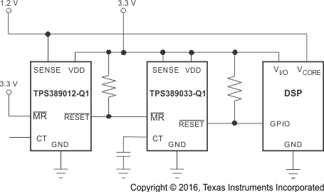
The manual reset (MR) input allows a processor or other logic circuits to initiate a reset. A logic low on MR causes RESET to assert. After MR returns to a logic high and SENSE is above VITP, RESET is deasserted after the user-defined reset delay. If MR is not controlled externally, then MR must be connected to VDD. Note that if the logic signal driving MR is not greater than or equal to VDD, then some additional current flows into VDD and out of MR and the difference is apparent when comparing Figure 8 and Figure 9.

Figure 23 shows how MR can be used to monitor multiple system voltages when only a single CT capacitor is needed to set the RESET delay time.
TPS3890-Q1 fbd_mr_monitor_volts_sbvs303.gifFigure 23. Using MR to Monitor Multiple System Voltages