SBVS172B July 2011 – April 2015
PRODUCTION DATA.
- 1 Features
- 2 Applications
- 3 Description
- 4 Revision History
- 5 Device Comparison Table
- 6 Pin Configuration and Functions
- 7 Specifications
- 8 Detailed Description
- 9 Applications and Implementation
- 10Power Supply Recommendations
- 11Layout
- 12Device and Documentation Support
- 13Mechanical, Packaging, and Orderable Information
Package Options
Mechanical Data (Package|Pins)
- DRY|6
Thermal pad, mechanical data (Package|Pins)
- DRY|6
Orderable Information
8 Detailed Description
8.1 Overview
The TPS3895, TPS3896, TPS3897, and TPS3898 devices (TPS389x) are a family of ultra-small supervisory circuits. The TPS389x is designed to assert the SENSE_OUT or SENSE_OUT signal, as shown in Table 1 and Table 2. When the SENSE pin rises above 0.5 V and the enable input is asserted (ENABLE = high or ENABLE = low) , the output asserts (SENSE_OUT goes high or SENSE_OUT goes low) after the capacitor-adjustable delay time. The SENSE pin can be set to any voltage threshold above 0.5 V using an external resistor divider. A broad range of output delay times and voltage thresholds can be supported, allowing these devices to be used in wide array of applications.
Table 1. TPS3895/7 Truth Table
| CONDITIONS | OUTPUT | STATUS | |
|---|---|---|---|
| ENABLE = high | SENSE < VIT+ | SENSE_OUT = low | Output not asserted |
| ENABLE = low | SENSE < VIT+ | SENSE_OUT = low | Output not asserted |
| ENABLE = low | SENSE > VIT+ | SENSE_OUT = low | Output not asserted |
| ENABLE = high | SENSE > VIT+ | SENSE_OUT = high | Output asserted after delay |
Table 2. TPS3896/8 Truth Table
| CONDITIONS | OUTPUT | STATUS | |
|---|---|---|---|
| ENABLE = low | SENSE < VIT+ | SENSE_OUT = high | Output not asserted |
| ENABLE = high | SENSE < VIT+ | SENSE_OUT = high | Output not asserted |
| ENABLE = high | SENSE > VIT+ | SENSE_OUT = high | Output not asserted |
| ENABLE = low | SENSE > VIT+ | SENSE_OUT = low | Output asserted after delay |
8.2 Functional Block Diagram
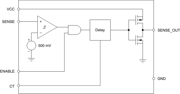 Figure 18. TPS3895A Block Diagram
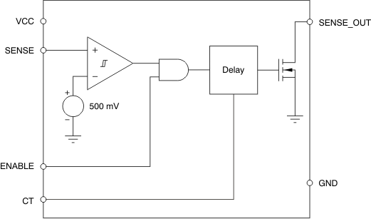 Figure 19. TPS3897A Block Diagram
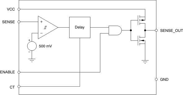 Figure 20. TPS3895P Block Diagram
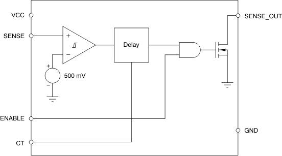 Figure 21. TPS3897P Block Diagram
8.3 Feature Description
8.3.1 Input Pin (SENSE)
The SENSE input pin allows any system voltage above 0.5 V to be monitored. If the voltage at the SENSE pin exceeds VIT+, and provided that the enable pin is asserted (ENABLE = high or ENABLE = low), then the output is asserted after the capacitor-adjustable delay time elapses. When the voltage at the SENSE pin drops below (VIT+ – Vhys), then the output is deasserted. The comparator has a built-in hysteresis to ensure smooth output assertions and deassertions. Although not required in most cases, for extremely noisy applications, it is good analog design practice to place a 1-nF to 10-nF bypass capacitor at the SENSE input in order to reduce sensitivity to transients and layout parasitics.
The TPS389x family monitor the voltage at SENSE with the use of external resistor divider, as shown in Figure 22.
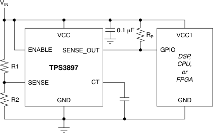 Figure 22. Using TPS3897 to Monitor User-Defined Threshold Voltage
The target threshold voltage can be calculated by using Equation 1:
When the input voltage (VIN) shown in Figure 22 is greater than VTARGET, then the output is asserted, provided that the enable pin is asserted (ENABLE = high or ENABLE = low). R1 and R2 can have high values (> 100 kΩ) to minimize current consumption as a result of a low SENSE input current without adding significant error to the resistive divider. Refer to application note SLVA450 to learn more about sizing sense-point resistors.
8.3.2 Enable Pin (ENABLE)
The enable input allows an external logic signal from other processors, logic circuits, and/or discrete sensors to turn on or turn off the output. The TPS3895 and TPS3897 offer an active-high enable input (ENABLE). The TPS3896 and TPS3898 offer an active-low enable input (ENABLE). Driving ENABLE low (or ENABLE high) forces SENSE_OUT to go low (or SENSE_OUT to go high). The 0.4-V (maximum) low and 1.4-V (minimum) high allow ENABLE to be driven with a 1.5-V or greater system supply.
The TPS389x family is available in two versions: the TPS389xA and TPS389xP. For TPS389xA devices with VSENSE > VIT+, driving ENABLE high (or ENABLE = low) makes SENSE_OUT go high (or SENSE_OUT go low) after the capacitor-adjustable delay time. For the TPS389xP versions with VSENSE > VIT+, driving ENABLE high (or ENABLE low) makes SENSE_OUT go high (or SENSE_OUT go low) after a 0.2-µs delay.
8.3.3 Output Pin (SENSE_OUT)
In a typical TPS389x application, the SENSE_OUT or SENSE_OUT outputs are connected to a reset/enable input of the processor (DSP, CPU, FPGA, ASIC, and so on) or connected to the enable input of a voltage regulator.
The TPS3897 and TPS3898 provide open-drain outputs. Pullup resistors must be used to hold these lines high when SENSE_OUT is asserted or SENSE_OUT is not asserted. By connecting the pullup resistors to the proper voltage rails, SENSE_OUT or SENSE_OUT can be connected to other devices at the correct interface voltage levels. The outputs can be pulled up to 18 V independent of the supply voltage (VCC). To ensure proper voltage levels, some thought should be given to choosing the correct pullup resistor values. The ability to sink current is determined by the supply voltage; therefore, if VCC = 5 V and the desired output pullup is 18 V, then to obtain a sink current of 1 mA or less (as mentioned in the Electrical Characteristics), the pullup resistor value should be greater than 18 kΩ. By using wired-OR logic, any combination of SENSE_OUT can be merged into one logic signal.
The TPS3895 and TPS3896 provide push-pull outputs. The logic high level of the outputs is determined by the VCC pin voltage. With this configuration, pullup resistors are not required and some board area can be saved. However, all the interface logic levels must be examined. All the SENSE_OUT and SENSE_OUT connections must be compatible with the VCC pin logic level.
The SENSE_OUT or SENSE_OUT outputs are defined for a VCC voltage higher than 0.8 V. Table 1 and Table 2 are truth tables that describe how the outputs are asserted or deasserted. When the conditions are met, the device changes state from deasserted to asserted after a preconfigured delay time. However, the transitions from asserted to deasserted are performed almost immediately with minimal propagation delay of 16 µs (typical). Figure 1 to Figure 4 show the timing diagrams and describe the relationship between the threshold voltages (VIT+ and Vhys), enable inputs, and respective outputs.
8.3.4 Output Delay Time Pin (CT)
To program a user-defined, adjustable delay time, an external capacitor must be connected between the CT pin and GND. If the CT pin is left open, there will be a delay of 40 µs. The adjustable delay time can be calculated through Equation 2:
The reset delay time is determined by the time it takes an on-chip, precision 310-nA current source to charge the external capacitor to 1.24 V. When SENSE > VIT+ and with ENABLE high (or ENABLE low), the internal current sources are enabled and begin to charge the external capacitors. When the CTn voltage on a capacitor reaches 1.24 V, the corresponding SENSE_OUT or SENSE_OUT is asserted. Note that a low-leakage type capacitor (such as ceramic) should be used, and that stray capacitance around this pin may cause errors in the reset delay time.
8.3.5 Immunity To Sense Pin Voltage Transients
The TPS389x is relatively immune to short negative transients on the SENSE pin. Sensitivity to transients depends on threshold overdrive, as shown in the typical characteristic graph Minimum Pulse Duration vs Threshold Overdrive Voltage (Figure 9).
8.4 Device Functional Modes
8.4.1 Normal Operation (VDD > VDD(min))
When the voltage on VDD is greater than VDD(min), the output corresponds to the voltages on the VDD and ENABLE pins relative to VIT–.
8.4.2 Below VDD(min) (V(POR) < VDD < VDD(min))
When the voltage on VDD is less than VDD(min) but greater than the power-on reset voltage (V(POR)), the output is deasserted (VSENSE_OUT is low and VSENSE_OUT is high.
8.4.3 Below Power-On Reset (VDD < V(POR))
When the voltage on VDD is lower than the power-on reset voltage (V(POR)), the output is undefined. Do not rely on the output for proper device function under this condition.