SLVSB90C January 2012 – November 2023 TPS40170-Q1
PRODUCTION DATA
- 1
- 1 Features
- 2 Applications
- 3 Description
- 4 Pin Configuration and Functions
- 5 Specifications
-
6 Detailed Description
- 6.1 Overview
- 6.2 Functional Block Diagram
- 6.3
Feature Description
- 6.3.1 LDO Linear Regulators and Enable
- 6.3.2 Input Undervoltage Lockout (UVLO)
- 6.3.3 Equations for Programming the Input UVLO
- 6.3.4 Overcurrent Protection and Short-Circuit Protection (OCP and SCP)
- 6.3.5 Oscillator and Voltage Feed-Forward
- 6.3.6 Feed-Forward Oscillator Timing Diagram
- 6.3.7 Soft-Start and Fault-Logic
- 6.3.8 Overtemperature Fault
- 6.3.9 Tracking
- 6.3.10 Adaptive Drivers
- 6.3.11 Start-Up Into Pre-Biased Output
- 6.3.12 31
- 6.3.13 Power Good (PGOOD)
- 6.3.14 PGND and AGND
- 6.3.15 Bootstrap Capacitor
- 6.3.16 Bypass and Filtering
- 6.4 Device Functional Modes
-
7 Application and Implementation
- 7.1 Application Information
- 7.2
Typical Application
- 7.2.1 Design Requirements
- 7.2.2
Detailed Design Procedure
- 7.2.2.1 Select A Switching Frequency
- 7.2.2.2 Inductor Selection (L1)
- 7.2.2.3 Output Capacitor Selection (C9)
- 7.2.2.4 Peak Current Rating of Inductor
- 7.2.2.5 Input Capacitor Selection (C1, C6)
- 7.2.2.6 MOSFET Switch Selection (Q1, Q2)
- 7.2.2.7 Timing Resistor (R7)
- 7.2.2.8 UVLO Programming Resistors (R2, R6)
- 7.2.2.9 Bootstrap Capacitor (C7)
- 7.2.2.10 VIN Bypass Capacitor (C18)
- 7.2.2.11 VBP Bypass Capacitor (C19)
- 7.2.2.12 SS Timing Capacitor (C15)
- 7.2.2.13 ILIM Resistor (R19, C17)
- 7.2.2.14 SCP Multiplier Selection (R5)
- 7.2.2.15 Feedback Divider (R10, R11)
- 7.2.2.16 Compensation: (R4, R13, C13, C14, C21)
- 7.2.3 Application Curves
- 7.3 Power Supply Recommendations
- 7.4 Layout
- 8 Device and Documentation Support
- 9 Revision History
- 10Mechanical, Packaging, and Orderable Information
Package Options
Mechanical Data (Package|Pins)
- RGY|20
Thermal pad, mechanical data (Package|Pins)
- RGY|20
Orderable Information
3 Description
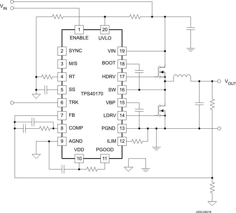
The TPS40170-Q1 device is a full-featured, synchronous PWM buck controller that operates at an input voltage between 4.5 V and 60 V and is optimized for high-power-density, high-reliability dc-dc converter applications. The controller implements voltage-mode control with input-voltage feed-forward compensation that enables instant response to an input voltage change. The switching frequency is programmable from 100 kHz to 600 kHz.
The TPS40170-Q1 device has a complete set of system protection and monitoring features such as programmable UVLO, programmable overcurrent protection (OCP) by sensing the low-side FET, selectable short-circuit protection (SCP) by sensing the high-side FET, and thermal shutdown. The ENABLE pin allows for system shutdown in a low-current (1-µA typical) mode. The controller supports pre-biased output, provides an open-drain PGOOD signal, and has closed-loop soft-start, output-voltage tracking, and adaptive dead-time control.
The TPS40170-Q1 device provides accurate output-voltage regulation within 1% accuracy. Additionally, the controller implements a novel scheme of bidirectional synchronization with one controller acting as the primary and other downstream controllers acting as secondaries, synchronized to the primary in-phase or 180° out-of-phase. Secondary controllers can be synchronized to an external clock within ±30% of the free-running switching frequency.
New products (LM5145-Q1 and LM5146-Q1) offer reduced BOM cost, higher efficiency, and reduced design size among many other features.
| PART NUMBER | PACKAGE(1) | PACKAGE SIZE (2) |
|---|---|---|
| TPS40170-Q1 | RGY (VQFN, 20) | 4.50 mm × 3.50 mm |
 Simplified Schematic