SLVS753C February 2007 – November 2016 TPS40180
PRODUCTION DATA.
- 1 Features
- 2 Applications
- 3 Description
- 4 Revision History
- 5 Pin Configuration and Functions
- 6 Specifications
-
7 Detailed Description
- 7.1 Overview
- 7.2 Functional Block Diagram
- 7.3
Feature Description
- 7.3.1 Current Sensing and Overcurrent Detection
- 7.3.2 Hiccup Fault Recovery
- 7.3.3 Selecting Current Sense Network Components
- 7.3.4 PGOOD Functionality
- 7.3.5 Output Overvoltage and Undervoltage Protection
- 7.3.6 Overtemperature Protection
- 7.3.7 eTRIM™
- 7.3.8 Connections Between Controllers for Stacking
- 7.3.9 VSH Line in the Multiphase
- 7.4 Device Functional Modes
- 7.5 Programming
-
8 Application and Implementation
- 8.1 Application Information
- 8.2
Typical Applications
- 8.2.1
Single Output Synchronous Buck Converter
- 8.2.1.1 Design Requirements
- 8.2.1.2
Detailed Design Procedure
- 8.2.1.2.1 Inductor Selection
- 8.2.1.2.2 Output Capacitor Selection
- 8.2.1.2.3 Input Capacitor Selection
- 8.2.1.2.4 MOSFET Selection
- 8.2.1.2.5
Peripheral Component Design
- 8.2.1.2.5.1 Switching Frequency Setting (RT)
- 8.2.1.2.5.2 Output Voltage Setting (FB)
- 8.2.1.2.5.3 Current Sensing Network Design (CS+, CS-)
- 8.2.1.2.5.4 Overcurrent Protection (ILIM)
- 8.2.1.2.5.5 VREG (PVCC)
- 8.2.1.2.5.6 BP5
- 8.2.1.2.5.7 Phase Select (PSEL)
- 8.2.1.2.5.8 VSHARE (VSH)
- 8.2.1.2.5.9 Powergood (PGOOD)
- 8.2.1.2.5.10 Undervoltage Lockout (UVLO)
- 8.2.1.2.5.11 Clock Synchronization (CLKIO)
- 8.2.1.2.5.12 Bootstrap Capacitor
- 8.2.1.2.5.13 Soft Start (SS)
- 8.2.1.2.5.14 Remote Sense
- 8.2.1.2.5.15 Feedback Compensator Design
- 8.2.1.3 Application Curves
- 8.2.2 Simultaneous Tracking With TPS40180 Devices
- 8.2.3 2-Phase Single Output With TPS40180
- 8.2.1
Single Output Synchronous Buck Converter
- 9 Power Supply Recommendations
- 10Layout
- 11Device and Documentation Support
- 12Mechanical, Packaging, and Orderable Information
Package Options
Mechanical Data (Package|Pins)
- RGE|24
Thermal pad, mechanical data (Package|Pins)
- RGE|24
Orderable Information
6 Specifications
6.1 Absolute Maximum Ratings
over operating free-air temperature range (unless otherwise noted)(1)| MIN | MAX | UNIT | ||
|---|---|---|---|---|
| Input voltage, VI | VDD, UVLO, RT, SS | –0.3 | 16 | V |
| FB, VOUT, GSNS, VSH, ILIM, BP5, PSEL, CS+, CS–, VS+, VS– | –0.3 | 6 | ||
| Output voltage, VO | BOOT – HDRV | –0.3 | 6 | V |
| SW, HDRV | –1 | 44 | ||
| SW, HDRV, transient (<50 ns) | –5 | 44 | ||
| DIFFO, LDRV, PVCC, CLKIO, PGOOD, COMP | –0.3 | 6 | ||
| PGOOD (eTrim™ usage only) | –0.3 | 22 | ||
| Operating junction temperature, TJ | –40 | 150 | °C | |
| Storage temperature, Tstg | –55 | 150 | °C | |
(1) Stresses beyond those listed under Absolute Maximum Ratings may cause permanent damage to the device. These are stress ratings only, which do not imply functional operation of the device at these or any other conditions beyond those indicated under Recommended Operating Conditions. Exposure to absolute-maximum-rated conditions for extended periods may affect device reliability.
6.2 ESD Ratings
| VALUE | UNIT | |||
|---|---|---|---|---|
| V(ESD) | Electrostatic discharge | Human-body model (HBM), per ANSI/ESDA/JEDEC JS-001(1) | ±2500 | V |
| Charged-device model (CDM), per JEDEC specification JESD22-C101(2) | ±1500 | |||
(1) JEDEC document JEP155 states that 500-V HBM allows safe manufacturing with a standard ESD control process.
(2) JEDEC document JEP157 states that 250-V CDM allows safe manufacturing with a standard ESD control process.
6.3 Recommended Operating Conditions
over operating free-air temperature range (unless otherwise noted)| MIN | NOM | MAX | UNIT | |||
|---|---|---|---|---|---|---|
| VI | Input voltage | VDD, UVLO | 4.5 | 15 | V | |
| SW | –1 | 40 | ||||
| BOOT – SW | 5.5 | |||||
| All other pins | 0 | 5.8 | ||||
| RT | 25 | µA | ||||
| PSEL | 150 | µA | ||||
| TJ | Operating junction temperature | –40 | 105 | °C | ||
6.4 Thermal Information
| THERMAL METRIC(1) | TPS40180 | UNIT | |
|---|---|---|---|
| RGE (VQFN) | |||
| 24 PINS | |||
| RθJA | Junction-to-ambient thermal resistance | 33.9 | °C/W |
| RθJC(top) | Junction-to-case (top) thermal resistance | 34.4 | °C/W |
| RθJB | Junction-to-board thermal resistance | 11.6 | °C/W |
| ψJT | Junction-to-top characterization parameter | 0.4 | °C/W |
| ψJB | Junction-to-board characterization parameter | 11.7 | °C/W |
| RθJC(bot) | Junction-to-case (bottom) thermal resistance | 3 | °C/W |
(1) For more information about traditional and new thermal metrics, see the Semiconductor and IC Package Thermal Metrics application report.
6.5 Electrical Characteristics
VVDD = 12 V, VBP5 = 15 V, VPVCC = 5 V, –40°C ≤ TJ ≤ 85°C (unless otherwise noted)| PARAMETER | TEST CONDITIONS | MIN | TYP | MAX | UNIT | |
|---|---|---|---|---|---|---|
| VDD INPUT SUPPLY | ||||||
| VVDD | Operating voltage range | 4.5 | 12 | 15 | V | |
| IVDDSD | Shutdown current | VUVLO < 0.5 V | 50 | µA | ||
| BP5 INPUT SUPPLY | ||||||
| VBP5 | Operating voltage range | 4.3 | 5 | 5.5 | V | |
| IBP5 | Operating current | 2 | 3 | 5 | mA | |
| VBP5UV | Rising undervoltage turn on threshold |
4 | 4.25 | 4.5 | V | |
| VBP5UVH | BP5 UVLO hysteresis | 225 | mV | |||
| PVCC REGULATOR | ||||||
| VPVCC | Output voltage | 4.5 V < VDD < 15 V | 4.3 | 5 | 5.5 | V |
| IPVCC | Output current | 0 | 50 | mA | ||
| OSCILLATOR | ||||||
| FOSC | Oscillator frequency | RRT = 64.9 kΩ | 360 | 415 | 454 | kHz |
| Oscillator frequency range | 150 | 1000 | ||||
| VRMP | Ramp voltage(1) | 420 | 500 | 525 | mV | |
| VRTCKLSLV | RT pin clock slave voltage threshold | 2 | V | |||
| DIGITAL CLOCK SIGNAL (CLKIO) | ||||||
| RCLKH | Pull up resistance(1) | 27 | Ω | |||
| RCLKL | Pull down resistance(1) | 27 | Ω | |||
| ICLKIOLK | Leakage current in high impedance state(1) |
VRT < 2 V, VPSEL = 5 V | 1 | µA | ||
| UVLO PIN | ||||||
| VUVLO(on) | PVCC regulator enabled | 0.8 | 0.9 | 1.5 | V | |
| PWM switching enabled | 1.9 | 2 | 2.1 | |||
| IUVLO | Hysteresis bias current | 9 | 12 | 15 | µA | |
| PULSE WIDTH MODULATOR | ||||||
| DMAX | Maximum duty cycle | 8 phase CLK scheme | 87.5% | |||
| 6 phase CLK scheme | 83% | |||||
| tON(min) | Minimum pulse width(1) | 75 | ns | |||
| VSHARE | ||||||
| VVSH | Current share reference; ramp valley voltage |
RLOAD = 20 kΩ | 1.7 | 1.8 | 1.9 | V |
| ERROR AMPLIFIER | ||||||
| IIB | Input bias current at FB pin | VFB = 0.7 V | –200 | 0 | 200 | nA |
| VREF | Trimmed FB control voltage | Includes differential sense amp offset | 695 | 700 | 705 | mV |
| IOH | COMP source current | VCOMP = 1.1 V, VFB = 0.6 V | 1 | 2 | mA | |
| IOL | COMP sink current | VCOMP = 1.1 V, VFB = 0.8 V | 1 | 2 | mA | |
| EAGBWP | Gain bandwidth product(1) | 8 | 12 | MHz | ||
| AOL | Open loop gain(1) | 60 | 90 | dB | ||
| SOFTSTART | ||||||
| ISS1 | Charging current (before first PWM pulse) |
Device enabled, during hiccup fault recovery |
6.5 | 7.5 | 8.2 | µA |
| ISS2 | Charging current (after first PWM pulse) |
12 | 15 | 17 | µA | |
| VSS_FE | Fault enable threshold | 0.8 | V | |||
| VSSSLV | Voltage loop slave mode threshold voltage |
VBP5 = 5 V | VBP5 – 0.75 | V | ||
| CURRENT LIMIT | ||||||
| IILIM | Threshold setting current | 21.5 | 23.5 | 25.5 | µA | |
| CURRENT SENSE AMPLIFIER | ||||||
| VISOFST | Input offset voltage | –2.5 | 0 | 2.5 | mV | |
| IIS_CS | Input bias current | 100 | nA | |||
| GCS | Gain at PWM input | 0.2 V ≤ VICM ≤ 5.8 V | 11.25 | 12.5 | 13.75 | V/V |
| VICM | Input common mode range | 0 | 5.8 | V | ||
| VDIFFMX | Maximum differential input voltage | –60 | 60 | mV | ||
| DIFFERENTIAL REMOVE VOLTAGE SENSE AMPLIFIER | ||||||
| GRVS | Gain | 0.7 V < V(VOUT) – V(GSNS) < 5.8 V | 0.995 | 1 | 1.005 | V/V |
| IDIFFOH | DIFFO source current | V(VOUT) – V(GSNS) = 2 V, V(DIFFO) > 1.98 V, V(VDD) – V(VOUT) > 2 V |
2 | mA | ||
| V(VOUT) – V(GSNS) = 5.8 V, V(DIFFO) > 5.6 V, V(VDD) – V(VOUT) > 1 V |
1 | |||||
| IDIFFOL | DIFFO sink current | V(VOUT) – V(GSNS) = 2 V, V(DIFFO) > 2.02 V |
2 | mA | ||
| BWDIFFA | Unity gain bandwidth(1) | 5 | 8 | MHz | ||
| RINDIFFA | Input resistance | Inverting, DIFFO to GSNS | 60 | kΩ | ||
| Noninverting, OUT to GND | 60 | |||||
| PSEL PIN | ||||||
| IISEL | Bias current | 21.5 | 23.5 | 25.5 | µA | |
| VMNCLK | Master mode | No output on CLKIO | 0 | 0 | 0.5 | V |
| VM8PH | 8 phase CLKIO | 0.5 | 0.7 | 0.9 | ||
| VM6PH | 6 phase CLKIO | 0.9 | ||||
| VSSTDBY | Slave mode, standby state | 3.4 | V | |||
| VS45 | Clock slave mode, 45° phase slot(1) |
8 phase CLKIO | 0 | 0 | 0.2 | V |
| VS90 | Clock slave mode, 90° phase slot(1) |
8 phase CLKIO | 0.2 | 0.35 | 0.5 | V |
| VS135 | Clock slave mode, 135° phase slot(1) |
8 phase CLKIO | 0.5 | 0.7 | 0.9 | V |
| VS180 | Clock slave mode, 180° phase slot(1) |
8 phase CLKIO | 0.9 | 1.1 | 1.3 | V |
| VS225 | Clock slave mode, 225° phase slot(1) |
8 phase CLKIO | 1.3 | 1.6 | 1.9 | V |
| VS270 | Clock slave mode, 270° phase slot(1) |
8 phase CLKIO | 1.9 | 2.25 | 2.6 | V |
| VS315 | Clock slave mode, 315° phase slot(1) |
8 phase CLKIO | 2.6 | 3 | 3.4 | V |
| VS0 | Clock slave mode, 0 phase slot(1) |
6 phase CLKIO | 1.9 | 2.25 | 2.6 | V |
| VS60 | Clock slave mode, 60° phase slot(1) |
6 phase CLKIO | 0 | 0 | 0.2 | V |
| VS120 | Clock slave mode, 120° phase slot(1) |
6 phase CLKIO | 0.2 | 0.35 | 0.5 | V |
| VS180 | Clock slave mode, 180° phase slot(1) |
6 phase CLKIO | 0.5 | 0.7 | 0.9 | V |
| VS240 | Clock slave mode, 240° phase slot(1) |
6 phase CLKIO | 0.9 | 1.1 | 1.3 | V |
| VS300 | Clock slave mode, 300° phase slot(1) |
6 phase CLKIO | 1.3 | 1.6 | 1.9 | V |
| GATE DRIVERS | ||||||
| RHDRV(on) | HDRV pull up resistance | VBOOT = 5 V, V(SW) = 0 V, IHDRV = 100 mA |
1 | 2 | 3 | Ω |
| RHDRV(off) | HDRV pull down resistance | VBOOT = 5 V, V(SW) = 0 V, IHDRV = 100 mA |
0.5 | 1 | 2 | Ω |
| RLDRV(on) | LDRV pull up resistance | VPVCC = 5 V, ILDRV = 100 mA | 1 | 2 | 3.5 | Ω |
| RLDRV(off) | LDRV pull down resistance | VPVCC = 5 V, ILDRV = 100 mA | 0.3 | 0.75 | 1.5 | Ω |
| tHDRV(r) | HDRV rise time(1) | CLOAD = 3.3 nF | 25 | 75 | ns | |
| tHDRV(f) | HDRV fall time(1) | CLOAD = 3.3 nF | 25 | 75 | ns | |
| tLDRV(r) | LDRV rise time(1) | CLOAD = 3.3 nF | 25 | 75 | ns | |
| tLDRV(f) | LDRV fall time(1) | CLOAD = 3.3 nF | 10 | 60 | ns | |
| POWER GOOD | ||||||
| VFBPG_H | Power good high FB voltage threshold | 764 | 787 | 798 | mV | |
| VFBPG_L | Power good low FB voltage threshold | 591 | 611 | 626 | mV | |
| VFBPG(hyst) | Power good threshold hysteresis | 30 | 60 | mV | ||
| TPGDLY | Power good delay time(1) | 10 | µs | |||
| VPGL | Power good low level output voltage | IPG = 2 mA | 0.35 | 0.4 | V | |
| IPGLK | Power good leakage current | VPG = 5 V | 1 | µA | ||
| OVERVOLTAGE AND UNDERVOLTAGE | ||||||
| VFB_U | FB pin under voltage threshold | 565 | 580 | 595 | mV | |
| VFB_O | FB pin over voltage threshold | 792 | 810 | 828 | mV | |
| THERMAL SHUTDOWN | ||||||
| TTSD | Shutdown temperature(1) | 126 | 135 | 144 | °C | |
| TTSD(hyst) | Hysteresis(1) | 40 | °C | |||
| TWRN | Warning temperature(1) | 106 | 115 | 124 | °C | |
| TWR(hyst) | Hysteresis(1) | 10 | °C | |||
(1) Specified by design. Not production tested.
6.6 Typical Characteristics
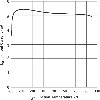 Figure 1. Input Shutdown Current vs Junction Temperature
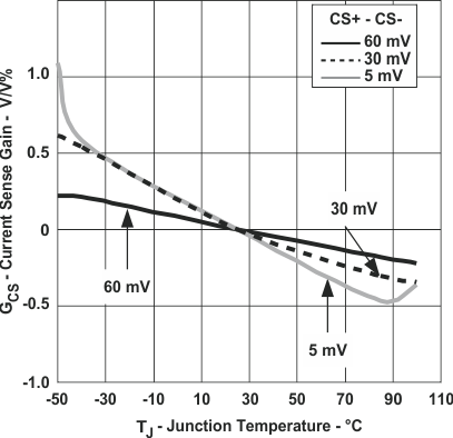 Figure 3. Relative Current Sense Gain
vs Junction Temperature
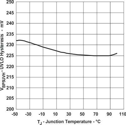 Figure 5. UVLO Hysteresis vs Junction Temperature
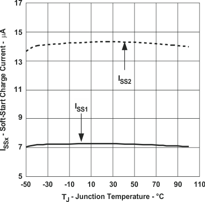 Figure 7. Soft-Start Charge Current vs Junction Temperature
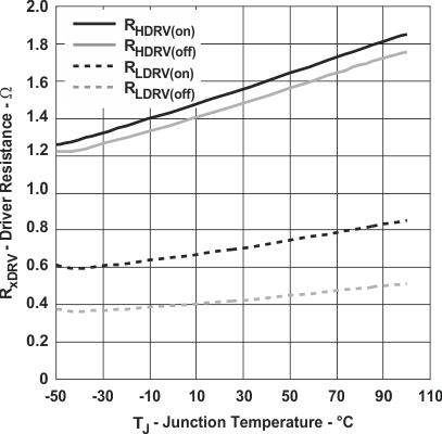 Figure 9. Driver Resistance vs Junction Temperature
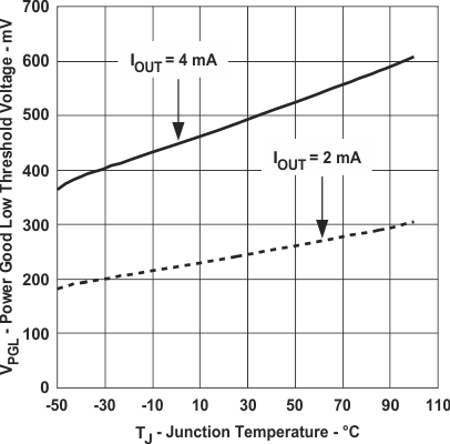 Figure 11. Power Good Low Threshold Voltage
vs Junction Temperature
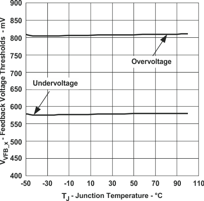 Figure 13. Undervoltage and Overvoltage Threshold
vs Junction Temperature
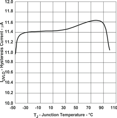 Figure 15. UVLO Hysteresis Current
vs Junction Temperature
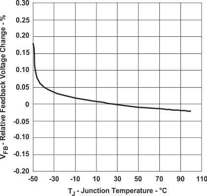 Figure 17. Relative Feedback Reference Voltage Change
vs Junction Temperature
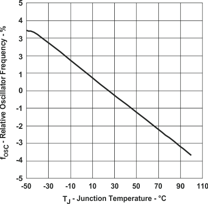 Figure 19. Relative Oscillator Frequency vs Junction Temperature
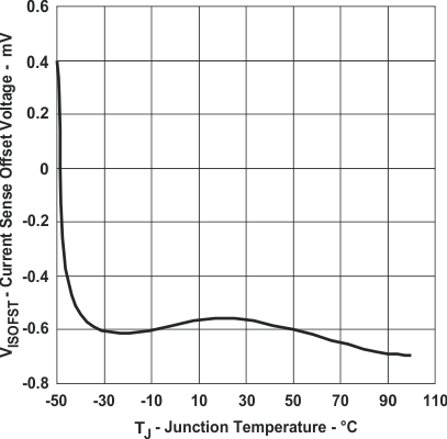 Figure 2. Current Sense Amplifier Offset Voltage
vs Junction Temperature
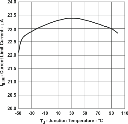 Figure 4. Current Limit vs Junction Temperature
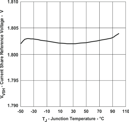 Figure 6. Current Share RE Voltage
vs Junction Temperature
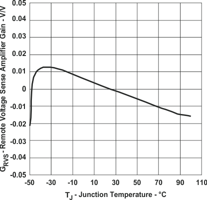 Figure 8. Remote Voltage Sense Amplifier
vs Junction Temperature
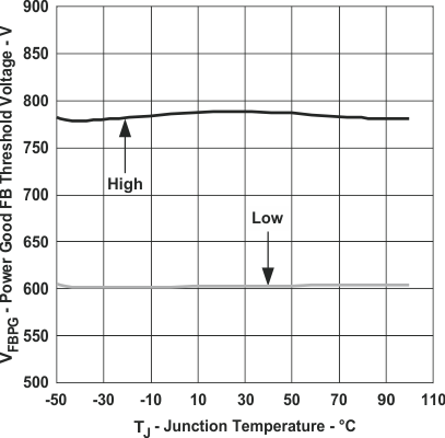 Figure 10. Power Good Threshold Voltage
vs Junction Temperature
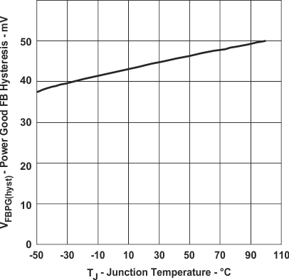 Figure 12. Power Good FB Hysteresis
vs Junction Temperature
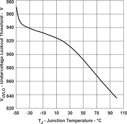 Figure 14. UVLO Enable Threshold vs Junction Temperature
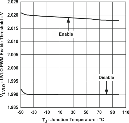 Figure 16. UVLO PWM Enable Threshold Voltage
vs Junction Temperature
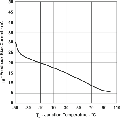 Figure 18. Feedback Bias Current vs Junction Temperature