SLUS720F February 2007 – June 2019 TPS40195
PRODUCTION DATA.
- 1 Features
- 2 Applications
- 3 Description
- 4 Revision History
- 5 Description (continued)
- 6 Pin Configuration and Functions
- 7 Specifications
- 8 Detailed Description
-
9 Application and Implementation
- 9.1 Application Information
- 9.2
Typical Applications
- 9.2.1
Typical Application 1
- 9.2.1.1 Design Requirements
- 9.2.1.2
Detailed Design Procedure
- 9.2.1.2.1 Output Inductor, LOUT
- 9.2.1.2.2 Output Capacitor, COUT
- 9.2.1.2.3 Input Capacitor, CIN
- 9.2.1.2.4 Switching MOSFET, QSW
- 9.2.1.2.5 Rectifier MOSFET, QSR
- 9.2.1.2.6
Component Selection for the TPS40195
- 9.2.1.2.6.1 Timing Resistor, RT
- 9.2.1.2.6.2 Setting UVLO
- 9.2.1.2.6.3 Setting the Soft-Start Time
- 9.2.1.2.6.4 Short-Circuit Protection, RILIM
- 9.2.1.2.6.5 Voltage Decoupling Capacitors, CBP, and CVDD
- 9.2.1.2.6.6 Boost Voltage, CBOOST and DBOOST (optional)
- 9.2.1.2.6.7 Closing the Feedback Loop RZ1, RP1, RPZ2, RSET1, RSET2, CZ2, CP2 AND CPZ1
- 9.2.1.2.7 Application Curve
- 9.2.2 Typical Application 2
- 9.2.3 Typical Application 3
- 9.2.1
Typical Application 1
- 10Layout
- 11Device and Documentation Support
- 12Mechanical, Packaging, and Orderable Information
Package Options
Mechanical Data (Package|Pins)
Thermal pad, mechanical data (Package|Pins)
- RGY|16
Orderable Information
8.3.1 Enable Functionality
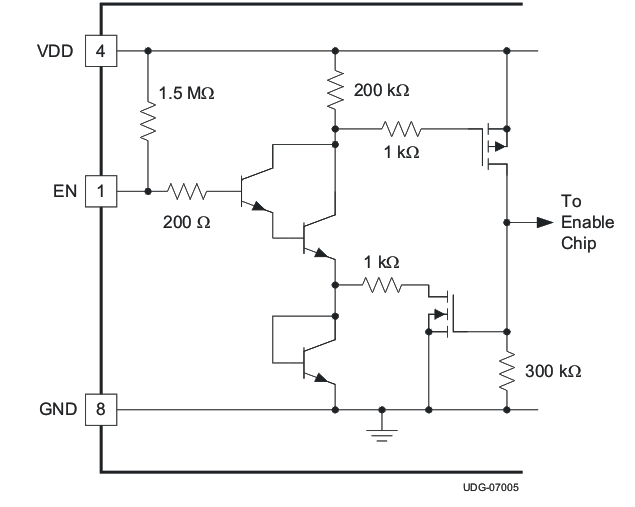
The TPS40195 has a dedicated device enable (EN) pin. This simplifies user level interface design since no multiplexed functions exist. Another benefit is a true low power shutdown mode of operation. When the EN pin is pulled to GND, all unnecessary functions inside the IC, including the BP regulator, are turned off and the TPS40195 consumes a typical 165-μA of current. A functionally equivalent circuit to the enable circuitry on the TPS40195 is shown in Figure 16.
 Figure 16. TPS40195 EN Pin Internal Circuitry
 If the EN pin is left floating, the chip starts automatically. The pin must be pulled to less than 600 mV for the TPS40195 to be in shutdown mode. Note that the EN pin is relatively high impedance. In some situations, there could be enough noise nearby to cause the EN pin to swing below the 600 mV threshold and give erroneous shutdown commands to the rest of the device. There are two solutions to this problem should it arise.
- Place a capacitor from EN to GND. A side effect of this is to delay the start of the converter while the capacitor charges past the enable threshold
- Place a resistor from VDD to EN. This causes more current to flow in the shutdown mode, but does not delay converter startup. If a resistor is used, the total current into the EN pin should be limited to no more than 500 μA.
The ENABLE pin is self-clamping. The clamp voltage can be as low as 1 V with a 1-kΩ ground impedance. Due to this self-clamping feature, the pull-up impedance on the ENABLE pin should be selected to limit the sink current to less than 500 μA. Driving the ENABLE pin with a low-impedance source voltage can result in damage to the device. Because of the self-clamping feature, it requires care when connecting multiple ENABLE pins together. For enabling multiple TPS4019x devices (TPS40190, TPS40192, TPS40193, TPS40195, TPS40197), see the Application Report SLVA509.
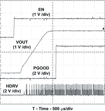
 Figure 17. TPS40195 EN Pin Start-up