SLUS720F February 2007 – June 2019 TPS40195
PRODUCTION DATA.
- 1 Features
- 2 Applications
- 3 Description
- 4 Revision History
- 5 Description (continued)
- 6 Pin Configuration and Functions
- 7 Specifications
- 8 Detailed Description
-
9 Application and Implementation
- 9.1 Application Information
- 9.2
Typical Applications
- 9.2.1
Typical Application 1
- 9.2.1.1 Design Requirements
- 9.2.1.2
Detailed Design Procedure
- 9.2.1.2.1 Output Inductor, LOUT
- 9.2.1.2.2 Output Capacitor, COUT
- 9.2.1.2.3 Input Capacitor, CIN
- 9.2.1.2.4 Switching MOSFET, QSW
- 9.2.1.2.5 Rectifier MOSFET, QSR
- 9.2.1.2.6
Component Selection for the TPS40195
- 9.2.1.2.6.1 Timing Resistor, RT
- 9.2.1.2.6.2 Setting UVLO
- 9.2.1.2.6.3 Setting the Soft-Start Time
- 9.2.1.2.6.4 Short-Circuit Protection, RILIM
- 9.2.1.2.6.5 Voltage Decoupling Capacitors, CBP, and CVDD
- 9.2.1.2.6.6 Boost Voltage, CBOOST and DBOOST (optional)
- 9.2.1.2.6.7 Closing the Feedback Loop RZ1, RP1, RPZ2, RSET1, RSET2, CZ2, CP2 AND CPZ1
- 9.2.1.2.7 Application Curve
- 9.2.2 Typical Application 2
- 9.2.3 Typical Application 3
- 9.2.1
Typical Application 1
- 10Layout
- 11Device and Documentation Support
- 12Mechanical, Packaging, and Orderable Information
Package Options
Mechanical Data (Package|Pins)
Thermal pad, mechanical data (Package|Pins)
- RGY|16
Orderable Information
7.6 Typical Characteristics
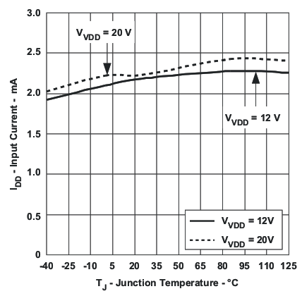 Figure 1. Input Current vs junction Temperature
 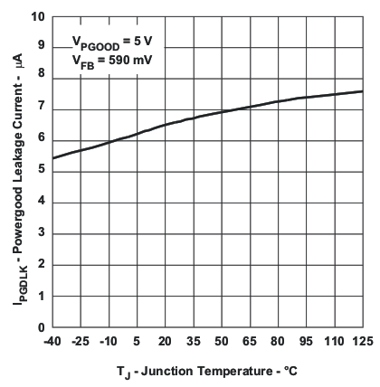 Figure 3. Powergood Leakage Current vs Junction Temperature
 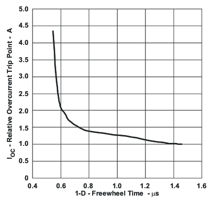 Figure 5. Relative Overcurrent Trip Point vs Freewheel Time
 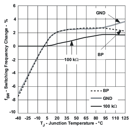 Figure 7. Switching Frequency Change vs Junction Temperature
 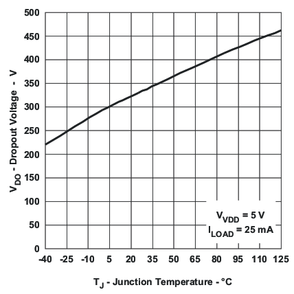 Figure 9. BP Dropout Voltage vs Junction Temperature
 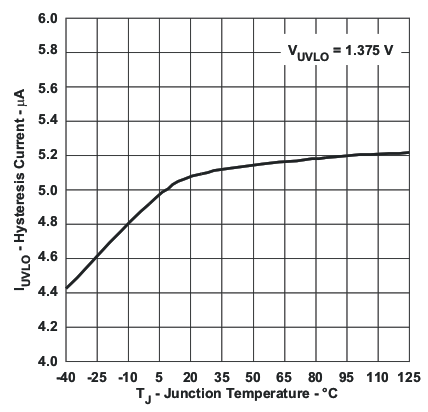 Figure 11. Undervoltage Lockout Hysteresis Vs Junction Temperature
 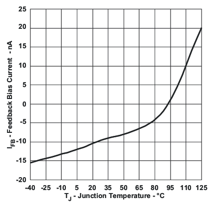 Figure 13. Feedback Bias Current vs Junction Temperature
 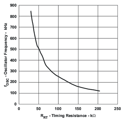 Figure 15. Oscillator Frequency vs Timing Resistance
 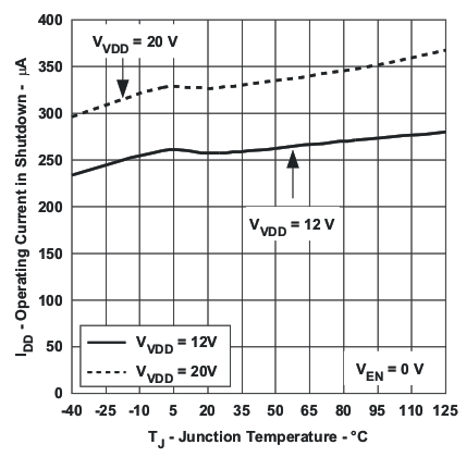 Figure 2. Operating Current in Shutdown vs Junction Temperature
 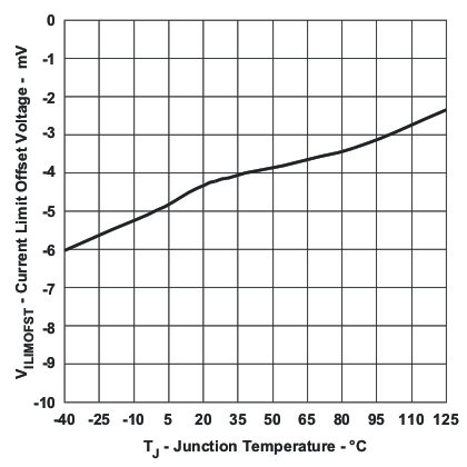 Figure 4. Current Limit Offset Voltage vs Junction Temperature
 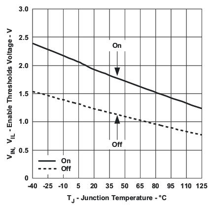 Figure 6. EN Threshold Voltages vs Junction Temperature
 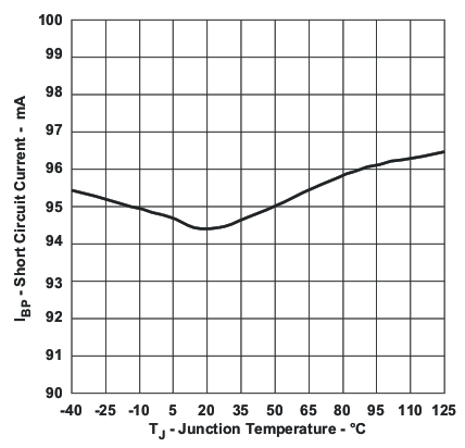 Figure 8. BP Short Circuit Current vs Junction Temperature
 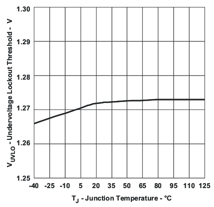 Figure 10. Undervoltage Lockout Threshold vs Junction Temperature
 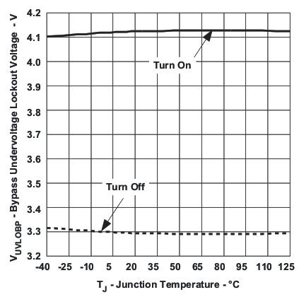 Figure 12. BP Undervoltage Lockout Voltage vs Junction Temperature
 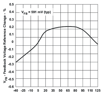 Figure 14. Relative Feedback Voltage Change vs Junction Temperature