SLUS720F February 2007 – June 2019 TPS40195
PRODUCTION DATA.
- 1 Features
- 2 Applications
- 3 Description
- 4 Revision History
- 5 Description (continued)
- 6 Pin Configuration and Functions
- 7 Specifications
- 8 Detailed Description
-
9 Application and Implementation
- 9.1 Application Information
- 9.2
Typical Applications
- 9.2.1
Typical Application 1
- 9.2.1.1 Design Requirements
- 9.2.1.2
Detailed Design Procedure
- 9.2.1.2.1 Output Inductor, LOUT
- 9.2.1.2.2 Output Capacitor, COUT
- 9.2.1.2.3 Input Capacitor, CIN
- 9.2.1.2.4 Switching MOSFET, QSW
- 9.2.1.2.5 Rectifier MOSFET, QSR
- 9.2.1.2.6
Component Selection for the TPS40195
- 9.2.1.2.6.1 Timing Resistor, RT
- 9.2.1.2.6.2 Setting UVLO
- 9.2.1.2.6.3 Setting the Soft-Start Time
- 9.2.1.2.6.4 Short-Circuit Protection, RILIM
- 9.2.1.2.6.5 Voltage Decoupling Capacitors, CBP, and CVDD
- 9.2.1.2.6.6 Boost Voltage, CBOOST and DBOOST (optional)
- 9.2.1.2.6.7 Closing the Feedback Loop RZ1, RP1, RPZ2, RSET1, RSET2, CZ2, CP2 AND CPZ1
- 9.2.1.2.7 Application Curve
- 9.2.2 Typical Application 2
- 9.2.3 Typical Application 3
- 9.2.1
Typical Application 1
- 10Layout
- 11Device and Documentation Support
- 12Mechanical, Packaging, and Orderable Information
Package Options
Mechanical Data (Package|Pins)
Thermal pad, mechanical data (Package|Pins)
- RGY|16
Orderable Information
8.3.4 Undervoltage Lockout (UVLO)
There are two separate UVLO circuits in the TPS40195. Both must be satisfied before the controller starts. One circuit detects the BP voltage and the other circuit detects voltage on the UVLO pin. The voltage on the BP pin (VBP) must be above 4.3 V in order for the device to start up.
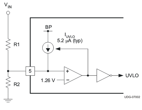
The UVLO pin is generally used to provide a higher UVLO voltage than that which the BP UVLO circuit provides. This level is programmed using a resistor divider from VIN to GND with the tap connected to the UVLO pin of the TPS40195. Hysteresis is provided by a 5.2-μA current source that is turned on when the UVLO pin reaches the 1.26 V turn on threshold. The turnon level is determined by the divider ratio, and the hysteresis level is determined by the divider equivalent impedance.
To determine the resistor values for the UVLO circuit, a turnon voltage and turn off voltage must be known. Once these are known the resistors can be calculated in Equation 2 and Equation 3. The functional schematic is shown in Figure 20.


where
- VON is the desired turnon voltage of the converter
- VOFF is the desired turn off voltage for the converter, must be less than VON
- IUVLO is the hysteresis current generated by the device, 5.2 μA (typical)
- VUVLO is the UVLO pin threshold voltage, 1.26 V (typical)
 Figure 20. Undervoltage Lockout