SLUS886B NOVEMBER 2008 – June 2019 TPS40197
PRODUCTION DATA.
- 1 Features
- 2 Applications
- 3 Description
- 4 Revision History
- 5 Description Continued
- 6 Pin Configuration and Functions
- 7 Specifications
- 8 Detailed Description
- 9 Application and Implementation
- 10Device and Documentation Support
- 11Mechanical, Packaging, and Orderable Information
Package Options
Mechanical Data (Package|Pins)
- RGY|16
Thermal pad, mechanical data (Package|Pins)
- RGY|16
Orderable Information
8.3.4 Start-up Sequence and Timing
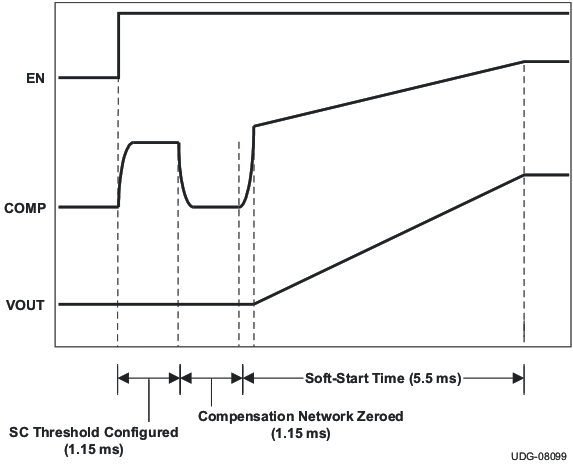
The TPS40197 startup sequence is as follows. After input power is applied, the 5-V onboard regulator initiates. Once this regulator comes up, the device goes through a period where it samples the impedance at the COMP pin and determines the short-circuit protection threshold voltage, by placing 400 mV on the COMP pin for approximately 1.15 ms. During this time, the current is measured and compared against internal thresholds to select the short circuit protection threshold. After this, the COMP pin is brought low for 1.15 ms. This ensures that the feedback loop is preconditioned at startup and no sudden output rise occurs at the output of the converter when the converter is allowed to start switching. After these initial 2.3 ms, the internal soft-start circuitry is engaged and the converter is allowed to start as shown in Figure 15.
 Figure 15. Start-up Sequence