SLUS886B NOVEMBER   2008  – June 2019 TPS40197

PRODUCTION DATA.  

  1. Features
  2. Applications
  3. Description
    1.     Device Images
      1.      Typical Application Circuit
  4. Revision History
  5. Description Continued
  6. Pin Configuration and Functions
    1.     Pin Functions
  7. Specifications
    1. 7.1 Absolute Maximum Ratings
    2. 7.2 ESD Ratings
    3. 7.3 Recommended Operating Conditions
    4. 7.4 Package Dissipation Ratings
    5. 7.5 Electrical Characteristics
    6. 7.6 Typical Characteristics
  8. Detailed Description
    1. 8.1 Overview
    2. 8.2 Functional Block Diagram
    3. 8.3 Feature Description
      1. 8.3.1  Enable
      2. 8.3.2  Oscillator
      3. 8.3.3  UVLO
      4. 8.3.4  Start-up Sequence and Timing
      5. 8.3.5  Selecting the Short Circuit Current
      6. 8.3.6  Voltage Reference and Dynamic VID
      7. 8.3.7  Minimum On-Time Consideration
      8. 8.3.8  BP Regulator
      9. 8.3.9  Prebias Start-up
      10. 8.3.10 Drivers
      11. 8.3.11 Power Good
      12. 8.3.12 Thermal Shutdown
  9. Application and Implementation
    1. 9.1 Application Information
    2. 9.2 Typical Application
      1. 9.2.1 Design Requirements
      2. 9.2.2 Detailed Design Procedure
  10. 10Device and Documentation Support
    1. 10.1 Device Support
      1. 10.1.1 Third-Party Products Disclaimer
    2. 10.2 Documentation Support
      1. 10.2.1 Related Devices
      2. 10.2.2 Related Documentation
    3. 10.3 Receiving Notification of Documentation Updates
    4. 10.4 Community Resources
    5. 10.5 Trademarks
    6. 10.6 Electrostatic Discharge Caution
    7. 10.7 Glossary
  11. 11Mechanical, Packaging, and Orderable Information

Package Options

Mechanical Data (Package|Pins)
Thermal pad, mechanical data (Package|Pins)
Orderable Information

Typical Application

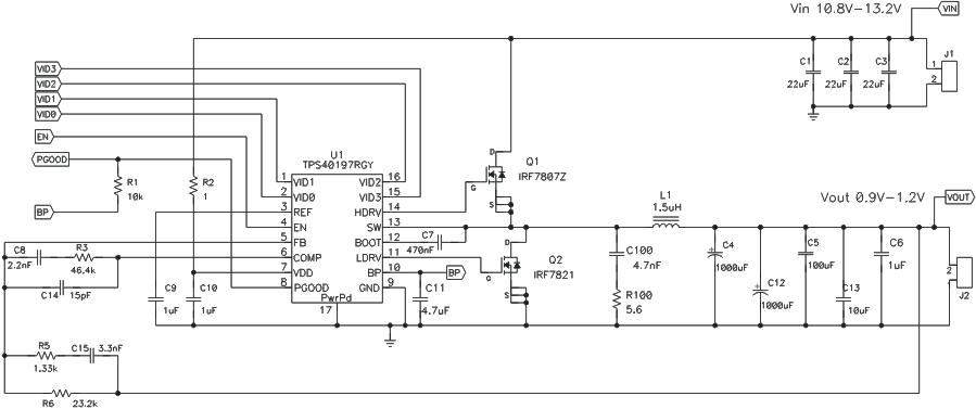
The schematic for the design is shown in Figure 17 and the list of materials is shown in Table 3.

TPS40197 de_schematic_lus853.gifFigure 17. TPS40197 Sample Schematic