SLUSC89 November 2015 TPS40210-EP
PRODUCTION DATA.
- 1 Features
- 2 Applications
- 3 Description
- 4 Revision History
- 5 Pin Configuration and Functions
- 6 Specifications
-
7 Detailed Description
- 7.1 Overview
- 7.2 Functional Block Diagram
- 7.3
Feature Description
- 7.3.1 Soft-Start
- 7.3.2 BP Regulator
- 7.3.3 Shutdown (DIS/EN Pin)
- 7.3.4 Minimum On-Time and Off-Time Considerations
- 7.3.5 Setting the Oscillator Frequency
- 7.3.6 Synchronizing the Oscillator
- 7.3.7 Current Sense and Overcurrent
- 7.3.8 Current Sense and Subharmonic Instability
- 7.3.9 Current Sense Filtering
- 7.3.10 Control Loop Considerations
- 7.3.11 Gate Drive Circuit
- 7.4 Device Functional Modes
-
8 Application and Implementation
- 8.1 Application Information
- 8.2
Typical Application
- 8.2.1 Design Requirements
- 8.2.2
Detailed Design Procedure
- 8.2.2.1 Duty Cycle Estimation
- 8.2.2.2 Inductor Selection
- 8.2.2.3 Rectifier Diode Selection
- 8.2.2.4 Output Capacitor Selection
- 8.2.2.5 Input Capacitor Selection
- 8.2.2.6 Current Sense and Current Limit
- 8.2.2.7 Current Sense Filter
- 8.2.2.8 Switching MOSFET Selection
- 8.2.2.9 Feedback Divider Resistors
- 8.2.2.10 Error Amplifier Compensation
- 8.2.2.11 RC Oscillator
- 8.2.2.12 Soft-Start Capacitor
- 8.2.2.13 Regulator Bypass
- 8.2.2.14 Bill of Materials
- 8.2.3 Application Curves
- 9 Power Supply Recommendations
- 10Layout
- 11Device and Documentation Support
- 12Mechanical, Packaging, and Orderable Information
Package Options
Mechanical Data (Package|Pins)
- DRC|10
Thermal pad, mechanical data (Package|Pins)
- DRC|10
Orderable Information
7 Detailed Description
7.1 Overview
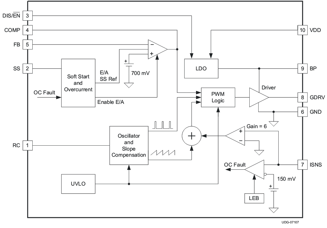
The TPS40210-EP is a peak current-mode control low-side controller with a built in 400-mA gate driver designed to drive N-channel MOSFETs at a fixed frequency. The frequency is adjustable from 35 kHz to 1000 kHz. Small size combined with complete functionality makes the part both versatile and easy to use.
The controller uses a low-value current-sensing resistor in series with the power MOSFET's source connection to detect switching current. When the voltage drop across this resistor exceeds 150 mV, the part enters an hiccup fault mode with a time period set by the external soft-start capacitor.
The TPS40210-EP uses voltage feedback to an error amplifier that is biased by a precision 700-mV reference. Internal slope compensation eliminates the characteristic sub-harmonic instability of peak current mode control with duty cycles of 50% or greater.
The TPS40210-EP also incorporates a soft-start feature where the output follows a slowly rising soft-start voltage, preventing output-voltage overshoot. The DIS/EN disables the TPS40210-EP putting it in a low quiescent current shutdown mode.
7.2 Functional Block Diagram
7.3 Feature Description
7.3.1 Soft-Start
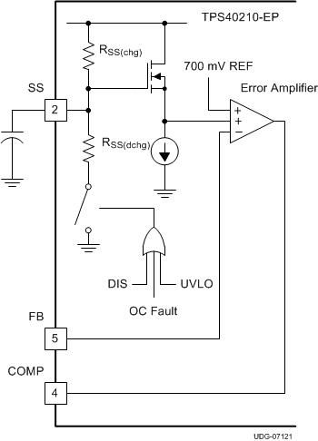
The soft-start feature of the TPS40210-EP is a closed-loop soft-start, meaning that the output voltage follows a linear ramp that is proportional to the ramp generated at the SS pin. This ramp is generated by an internal resistor connected from the BP pin to the SS pin and an external capacitor connected from the SS pin to GND. The SS pin voltage (VSS) is level shifted down by approximately VSS(ofst) (approximately 700 mV) and sent to one of the “+” (the “+” input with the lowest voltage dominates) inputs of the error amplifier. When this level shifted voltage (VSSE) starts to rise at time t1 (see Figure 20), the output voltage the controller expects, rises as well. Since VSSE starts at near 0 V, the controller attempts to regulate the output voltage from a starting point of zero volts. It cannot do this due to the converter architecture. The output voltage starts from the input voltage less the drop across the diode (VIN – VD) and rises from there. The point at which the output voltage starts to rise (t2) is the point where the VSSE ramp passes the point where it is commanding more output voltage than (VIN – VD). This voltage level is labeled VSSE(1). The time required for the output voltage to ramp from a theoretical zero to the final regulated value (from t1 to t3) is determined by the time it takes for the capacitor connected to the SS pin (CSS) to rise through a 700-mV range, beginning at VSS(ofst) above GND.
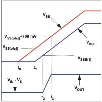
The required capacitance for a given soft-start time t3 – t1 in Figure 20 is calculated in Equation 1.

where
- tSS is the soft-start time, in seconds
- RSS(chg) is the SS charging resistance in Ω, typically 500 kΩ
- CSS is the value of the capacitor on the SS pin, in F
- VBP is the value of the voltage on the BP pin, in V
- VSS(ofst) is the approximate level shift from the SS pin to the error amplifier (~700 mV)
- VFB is the error amplifier reference voltage, 700 mV typical
Note that tSS is the time it takes for the output voltage to rise from 0 V to the final output voltage. Also note the tolerance on RSS(chg) given in the electrical specifications table. This contributes to some variability in the output voltage rise time and margin must be applied to account for it in design.
Also take note of VBP. Its value varies depending on input conditions. For example, a converter operating from a slowly rising input initializes VBP at a fairly low value and increases during the entire startup sequence. If the controller has a voltage above 8V at the input and the DIS pin is used to stop and then restart the converter, VBP is approximately 8V for the entire startup sequence. The higher the voltage on BP, the shorter the startup time is and conversely, the lower the voltage on BP, the longer the startup time is.
The soft-start time (tSS) must be chosen long enough so that the converter can start up without going into an overcurrent state. Since the over current state is triggered by sensing the peak voltage on the ISNS pin, that voltage must be kept below the overcurrent threshold voltage VISNS(oc). The voltage on the ISNS pin is a function of the load current of the converter, the rate of rise of the output voltage and the output capacitance, and the current sensing resistor. The total output current that must be supported by the converter is the sum of the charging current required by the output capacitor and any external load that must be supplied during startup. This current must be less than the IOUT(oc) value used in Equation 15 or Equation 16 (depending on the operating mode of the converter) to determine the current sense resistor value. In these equations, the actual input voltage at the time that the controller reaches the final output voltage is the important input voltage to use in the calculations. If the input voltage is slowly rising and is at less than the nominal input voltage when the startup time ends, the output current limit is less than IOUT(oc) at the nominal input voltage. The output capacitor charging current must be reduced (decrease COUT or increase the tSS) or IOUT(oc) must be increased and a new value for RISNS calculated.


where
- IC(chg) is the output capacitor charging current in A
- COUT is the total output capacitance in F
- VOUT is the output voltage in V
- tSS is the soft-start time from Equation 1
- IOUT(oc) is the desired over current trip point in A
- IEXT is any external load current in A
The capacitor on the SS pin (CSS) also plays a role in overcurrent functionality. It is used as the timer between restart attempts. The SS pin is connected to GND through a resistor, RSS(dchg), whenever the controller senses an overcurrent condition. Switching stops and nothing else happens until the SS pin discharges to the soft-start reset threshold, VSS(rst). At this point, the SS pin capacitor is allowed to charge again through the charging resistor RSS(chg), and the controller restarts from that point. The shortest time between restart attempts occurs when the SS pin discharges from VSS(ofst) (approximately 700 mV) to VSS(rst) (150 mV) and then back to VSS(ofst) and switching resumes. In actuality, this is a conservative estimate since switching does not resume until the VSSE ramp rises to a point where it is commanding more output voltage than exists at the output of the controller. This occurs at some SS pin voltage greater than VSS(ofst) and depends on the voltage that remains on the output overvoltage the converter while switching has been halted. The fastest restart time can be calculated by using Equation 4, Equation 5, and Equation 6.


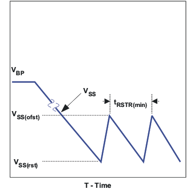 Figure 22. Soft-Start during Overcurrent
7.3.2 BP Regulator
The TPS40210-EP has an on board linear regulator the supplies power for the internal circuitry of the controller, including the gate driver. This regulator has a nominal output voltage of 8 V and must be bypassed with a 1-μF capacitor. If the voltage at the VDD pin is less than 8 V, the voltage on the BP pin will also be less and the gate drive voltage to the external FET is reduced from the nominal 8 V. This should be considered when choosing a FET for the converter.
Connecting external loads to this regulator can be done, but care must be taken to ensure that the thermal rating of the device is observed since there is no thermal shutdown feature in this controller. Exceeding the thermal ratings cause out of specification behavior and can lead to reduced reliability. The controller dissipates more power when there is an external load on the BP pin and is tested for dropout voltage for up to 5mA load. When the controller is in the disabled state, the BP pin regulator also shuts off so loads connected there power down as well. When the controller is disabled with the DIS/EN pin, this regulator is turned off.
The total power dissipation in the controller can be calculated as follows. The total power is the sum of PQ, PG, and PE.


where
- PQ is the quiescent power of the device in W
- VDD is the VDD pin voltage in V
- IDD(en) is the quiescent current of the controller when enabled but not switching in A
- PG is the power dissipated by driving the gate of the FET in W
- Qg is the total gate charge of the FET at the voltage on the BP pin in C
- f SW is the switching frequency in Hz
- PE is the dissipation caused be external loading of the BP pin in W
- IEXT is the external load current in A
7.3.3 Shutdown (DIS/EN Pin)
The DIS/EN pin is an active high shutdown command for the controller. Pulling this pin above 1.2 V causes the controller to completely shut down and enter a low current consumption state. In this state, the regulator connected to the BP pin is turned off. There is an internal 1.1-MΩ pulldown resistor connected to this pin that keeps the pin at GND level when left floating. If this function is not used in an application, it is best to connect this pin to GND.
7.3.4 Minimum On-Time and Off-Time Considerations
The TPS40210-EP has a minimum off-time of approximately 200 ns and a minimum on-time of 300 ns. These two constraints place limitations on the operating frequency that can be used for a given input to output conversion ratio. See Figure 2 for the maximum frequency that can be used for a given duty cycle.
The duty cycle at which the converter operates is dependent on the mode in which the converter is running. If the converter is running in discontinuous conduction mode, the duty cycle varies with changes to the load much more than it does when running in continuous conduction mode.
In continuous conduction mode, the duty cycle is related primarily to the input and output voltages.


In discontinuous mode the duty cycle is a function of the load, input and output voltages, inductance and switching frequency.

All converters using a diode as the freewheeling or catch component have a load current level at which they transition from discontinuous conduction to continuous conduction. This is the point where the inductor current just falls to zero. At higher load currents, the inductor current does not fall to zero but remains flowing in a positive direction and assumes a trapezoidal wave shape as opposed to a triangular wave shape. This load boundary between discontinuous conduction and continuous conduction can be found for a set of converter parameters as follows.

For loads higher than the result of Equation 13, the duty cycle is given by Equation 11 and for loads less that the results of Equation 13, the duty cycle is given Equation 12. For Equations 1 through 4, the variable definitions are as follows.
- VOUT is the output voltage of the converter in V
- VD is the forward conduction voltage drop across the rectifier or catch diode in V
- VIN is the input voltage to the converter in V
- IOUT is the output current of the converter in A
- L is the inductor value in H
- f SW is the switching frequency in Hz
7.3.5 Setting the Oscillator Frequency
The oscillator frequency is determined by a resistor and capacitor connected to the RC pin of the TPS40210-EP. The capacitor is charged to a level of approximately VDD/20 by current flowing through the resistor and is then discharged by a transistor internal to the TPS40210-EP. The required resistor for a given oscillator frequency is found from either Figure 1 or Equation 14.

where
- RT is the timing resistance in kΩ.
- ƒSW is the switching frequency in kHz.
- CT is the timing capacitance in pF.
For most applications a capacitor in the range of 68 pF to 120 pF gives the best results. Resistor values should be limited to between 100 kΩ and 1 MΩ as well. If the resistor value falls below 100 kΩ, decrease the capacitor size and recalculate the resistor value for the desired frequency. As the capacitor size decreases below 47 pF, the accuracy of Equation 14 degrades and empirical means may be needed to fine tune the timing component values to achieve the desired switching frequency.
7.3.6 Synchronizing the Oscillator
The TPS40210-EP can be synchronized to an external clock source. Figure 23 shows the functional diagram of the oscillator. When synchronizing the oscillator to an external clock, the RC pin must be pulled below 150 mV for 20 ns or more. The external clock frequency must be higher than the free running frequency of the converter as well. When synchronizing the controller, if the RC pin is held low for an excessive amount of time, erratic operation may occur. The maximum amount of time that the RC pin should be held low is 50% of a nominal output pulse, or 10% of the period of the synchronization frequency. If the external clock signal cannot operate with a low enough duty cycle to limit the amount of time the RC pin is held low, a resistor and capacitor can be added at the gate of the synchronization MOSFET. The capacitor should be added in series with the gate of the MOSFET to AC couple the rising edge of the synchronization signal. The resistor should be added from the gate of the MOSFET to ground to turn off the MOSFET. Typical values for the resistor and capacitor are 220 pF and 1 kΩ.
Under circumstances where the duty cycle is less than 50%, a Schottky diode connected from the RC pin to an external clock may be used to synchronize the oscillator. The cathode of the diode is connected to the RC pin. The trip point of the oscillator is set by an internal voltage divider to be 1/20 of the input voltage. The clock signal must have an amplitude higher than this trip point. When the clock goes low, it allows the reset current to restart the RC ramp, synchronizing the oscillator to the external clock. This provides a simple, single-component method for clock synchronization.
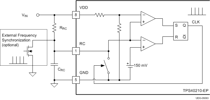 Figure 23. Oscillator Functional Diagram
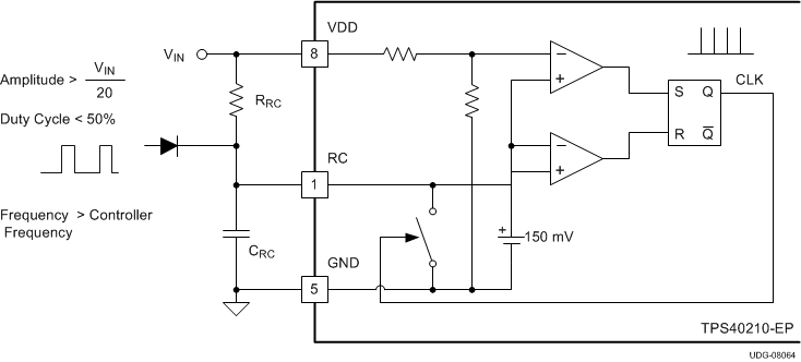 Figure 24. Diode Connected Synchronization
7.3.7 Current Sense and Overcurrent
The TPS40210-EP is a current mode controller that uses a resistor in series with the source terminal power FET to sense current for both the current mode control and overcurrent protection. The device enters a current limit state if the voltage on the ISNS pin exceeds the current limit threshold voltage VISNS(oc) from the electrical specifications table. When this happens the controller discharges the SS capacitor through a relatively high impedance and then attempt to restart. The amount of output current that causes this to happen is dependent on several variables in the converter.
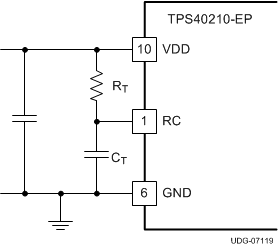
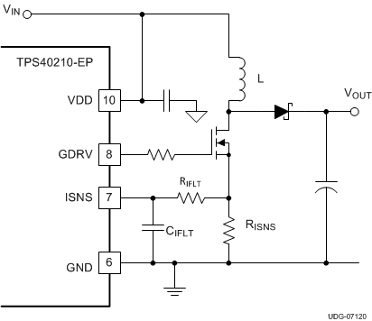
The load current overcurrent threshold is set by proper choice of RISNS. If the converter is operating in discontinuous mode the current sense resistor is found in Equation 15.

If the converter is operating in continuous conduction mode RISNS can be found in Equation 16.

where
- RISNS is the value of the current sense resistor in Ω.
- VISNS(oc) is the overcurrent threshold voltage at the ISNS pin (from electrical specifications).
- D is the duty cycle (from Equation 11).
- ƒSW is the switching frequency in Hz.
- VIN is the input voltage to the power stage in V (see text).
- L is the value of the inductor in H.
- IOUT(oc) is the desired overcurrent trip point in A.
- VD is the drop across the diode in Figure 26.
The TPS40210-EP has a fixed undervoltage lockout (UVLO) that allows the controller to start at a typical input voltage of 4.25 V. If the input voltage is slowly rising, the converter might have less than its designed nominal input voltage available when it has reached regulation. As a result, this may decreases the apparent current limit load current value and must be taken into consideration when selecting RISNS. The value of VIN used to calculate RISNS must be the value at which the converter finishes startup. The total converter output current at startup is the sum of the external load current and the current required to charge the output capacitors. See the Soft-Start for information on calculating the required output capacitor charging current.
The topology of the standard boost converter has no method to limit current from the input to the output in the event of a short circuit fault on the output of the converter. If protection from this type of event is desired, it is necessary to use some secondary protection scheme, such as a fuse, or rely on the current limit of the upstream power source.
7.3.8 Current Sense and Subharmonic Instability
A characteristic of peak current mode control results in a condition where the current control loop can exhibit instability. This results in alternating long and short pulses from the pulse width modulator. The voltage loop maintains regulation and does not oscillate, but the output ripple voltage increases. The condition occurs only when the converter is operating in continuous conduction mode and the duty cycle is 50% or greater. The cause of this condition is described in SLUA101, available at www.ti.com. The remedy for this condition is to apply a compensating ramp from the oscillator to the signal going to the pulse width modulator. In the TPS40210-EP the oscillator ramp is applied in a fixed amount to the pulse width modulator. The slope of the ramp is given in Equation 17.

To ensure that the converter does not enter into sub-harmonic instability, the slope of the compensating ramp signal must be at least half of the down slope of the current ramp signal. Since the compensating ramp is fixed in the TPS40210-EP, this places a constraint on the selection of the current sense resistor.
The down slope of the current sense wave form at the pulse width modulator is described in Equation 18.

Since the slope compensation ramp must be at least half, and preferably equal to the down slope of the current sense waveform seen at the pulse width modulator, a maximum value is placed on the current sense resistor when operating in continuous mode at 50% duty cycle or greater. For design purposes, some margin should be applied to the actual value of the current sense resistor. As a starting point, the actual resistor chosen should be 80% or less that the value calculated in Equation 19. This equation calculates the resistor value that makes the slope compensation ramp equal to one half of the current ramp downslope. Values no more than 80% of this result would be acceptable.

where
- Se is the slope of the voltage compensating ramp applied to the pulse width modulator in V/s.
- f SW is the switching frequency in Hz.
- VDD is the voltage at the VDD pin in V.
- m2 is the down slope of the current sense waveform seen at the pulse width modulator in V/s.
- RISNS is the value of the current sense resistor in Ω.
- VOUT is the converter output voltage VIN is the converter power stage input voltage.
- VD is the drop across the diode in Figure 26.
It is possible to increase the voltage compensation ramp slope by connecting the VDD pin to the output voltage of the converter instead of the input voltage as shown in Figure 26. This can help in situations where the converter design calls for a large ripple current value in relation to the desired output current limit setting.
NOTE
Connecting the VDD pin to the output voltage of the converter affects the startup voltage of the converter since the controller undervoltage lockout (UVLO) circuit monitors the VDD pin and senses the input voltage less the diode drop before startup. The effect is to increase the startup voltage by the value of the diode voltage drop.
If an acceptable RISNS value is not available, the next higher value can be used and the signal from the resistor divided down to an acceptable level by placing another resistor in parallel with CIFLT.
7.3.9 Current Sense Filtering
In most cases, a small filter placed on the ISNS pin improves performance of the converter. These are the components RIFLT and CIFLT in Figure 26. The time constant of this filter should be approximately 10% of the nominal pulse width of the converter. The pulse width can be found using Equation 20.

The suggested time constant is then

The range of RIFLT should be from about 1 kΩ to 5 kΩ for best results. Higher values can be used but this raises the impedance of the ISNS pin connection more than necessary and can lead to noise pickup issues in some layouts. CIFLT should be located as close as possible to the ISNS pin as well to provide noise immunity.
7.3.10 Control Loop Considerations
There are two methods to design a suitable control loop for the TPS40210-EP. The first and preferred if equipment is available is to use a frequency response analyzer to measure the open loop modulator and power stage gain and to then design compensation to fit that. The usage of these tools for this purpose is well documented with the literature that accompanies the tool and is not be discussed here.
The second option is to make an initial guess at compensation, and then evaluate the transient response of the system to see if the compensation is acceptable to the application or not. For most systems, an adequate response can be obtained by simply placing a series resistor and capacitor (RFB and CFB) from the COMP pin to the FB pin as shown in Figure 27. The initial compensation selection can be done more accurately with aid of WEBENCH® to select the components or the average Spice model to simulate the open loop modulator and power stage gain.
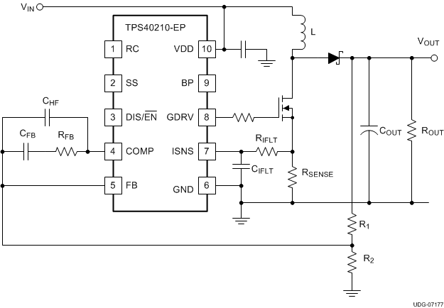 Figure 27. Basic Compensation Network
The natural phase characteristics of most capacitors used for boost outputs combined with the current mode control provide adequate phase margin when using this type of compensation. To determine an initial starting point for the compensation, the desired crossover frequency must be considered when estimating the control to output gain. The model used is a current source into the output capacitor and load.
When using these equations, the loop bandwidth should be no more than 20% of the switching frequency, ƒSW. A more reasonable loop bandwidth would be 10% of the switching frequency. Be sure to evaluate the transient response of the converter over the expected load range to ensure acceptable operation.


where
- KCO is the control to output gain of the converter, in V/V
- gM is the transconductance of the power stage and modulator, in S
- ROUT is the output load equivalent resistance, in Ω
- ZOUT is the output impedance, including the output capacitor, in Ω
- RISNS is the value of the current sense resistor, in Ω
- L is the value of the inductor, in H
- COUT is the value of the output capacitance, in F
- RESR is the equivalent series resistance of COUT, in Ω
- f SW is the switching frequency, in Hz
- f L is the desired crossover frequency for the control loop, in Hz
These equations assume that the operation is discontinuous and that the load is purely resistive. The gain in continuous conduction can be found by evaluating Equation 23 at the resistance that gives the critical conduction current for the converter. Loads that are more like current sources give slightly higher gains than predicted here. To find the gain of the compensation network required for a control loop of bandwidth ƒL, take the reciprocal of Equation 22.

The GBWP of the error amplifier is only guaranteed to be at least 1.5MHz. If KCOMP multiplied by ƒL is greater than 750 kHz, reduce the desired loop crossover frequency until this condition is satisfied. This ensures that the high-frequency pole from the error amplifier response with the compensation network in place does not cause excessive phase lag at ƒL and decreased phase margin in the loop.
The RC network connected from COMP to FB places a zero in the compensation response. That zero should be approximately 1/10th of the desired crossover frequency, ƒL. With that being the case, RFB and CFB can be found from Equation 26 and Equation 27


where
- R1 is the high side feedback resistor in Figure 27, in Ω
- ƒL is the desired loop crossover frequency, in Hz
Thought not strictly necessary, it is recommended that a capacitor be added between COMP and FB to provide high-frequency noise attenuation in the control loop circuit. This capacitor introduces another pole in the compensation response. The allowable location of that pole frequency determines the capacitor value. As a starting point, the pole frequency should be 10 × ƒL. The value of CHF can be found from Equation 28.

While the error amplifier GBWP will usually be higher, it can be as low as 1.5 MHz. If 10 × KComp × ƒL > 1.5 MHz, the error amplifier gain-bandwidth product may limit the high-frequency response below that of the high-frequency capacitor. To maintain a consistent high-frequency gain roll-off, CHF can be calculated by Equation 29.

where
- CHF is the high-frequency roll-off capacitor value in F
- RFB is the mid band gain setting resistor value in Ω
7.3.11 Gate Drive Circuit
Some applications benefit from the addition of a resistor connected between the GDRV pin and the gate of the switching MOSFET. In applications that have particularly stringent load regulation (under 0.75%) requirements and operate from input voltages above 5 V, or are sensitive to pulse jitter in the discontinuous conduction region, this resistor is recommended. The recommended starting point for the value of this resistor can be calculated from Equation 30.

where
- QG is the MOSFET total gate charge at 8V, VGS in nC
- RG is the suggested starting point gate resistance in Ω
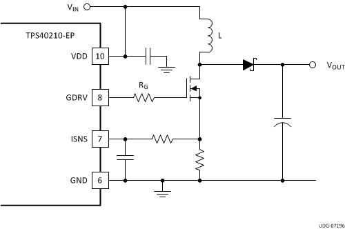 Figure 28. Gate Drive Resistor
7.4 Device Functional Modes
7.4.1 Operation Near Minimum Input Voltage
The TPS40210-EP is designed to operate with input voltages above 4.5 V. The typical VDD UVLO threshold is 4.25 V and the device may operate at input voltages down to the UVLO voltage. At input voltages below the actual UVLO voltage, the device will not switch. When VVDD passes the UVLO threshold the device will become active. Switching is enabled and the soft-start sequence is initiated. The TPS40210-EP will ramp up the output voltage at the rate determined by the external capacitor at the SS pin.
7.4.2 Operation With DIS/EN Pin
The DIS/EN pin has a 1.2-V typical threshold which can be used to disable the TPS40210-EP. With DIS/EN forced above this threshold voltage the device is disabled and switching is inhibited even if VVDD is above its UVLO threshold. Hysteresis on the DIS/EN pin threshold gives a typical turn-on threshold of 1.05 V. If the DIS/EN is left floating or is pulled below the 1.05-V threshold while VVDD is above its UVLO threshold, the device becomes active. Switching is enabled and the soft-start sequence is initiated. The TPS40210-EP will ramp up the output voltage at the rate determined by the external capacitor at the soft-start pin.