SLUSBO6C JANUARY 2014 – October 2018 TPS40425
PRODUCTION DATA.
- 1 Features
- 2 Applications
- 3 Description
- 4 Revision History
- 5 Pin Configuration and Functions
- 6 Specifications
-
7 Detailed Description
- 7.1 Overview
- 7.2 Functional Block Diagram
- 7.3
Feature Description
- 7.3.1 Asynchronous Pulse Injection (API)
- 7.3.2 Adaptive Voltage Scaling (AVS)
- 7.3.3 Switching Frequency and Synchronization
- 7.3.4 Voltage Reference
- 7.3.5 Output Voltage and Remote Sensing Amplifier
- 7.3.6 Current Sensing and Temperature Sensing Modes
- 7.3.7 Current Sensing
- 7.3.8 Temperature Sensing
- 7.3.9 Current Sharing
- 7.3.10 Linear Regulators
- 7.3.11 Power Sequence Between TPS40425 Device and Power Stage
- 7.3.12 PWM Signal
- 7.3.13 Startup and Shutdown
- 7.3.14 Pre-Biased Output Start-up
- 7.3.15 PGOOD Indication
- 7.3.16 Overcurrent Protection
- 7.3.17 Overvoltage/Undervoltage Protection
- 7.3.18 Overtemperature Fault Protection
- 7.3.19 Input Undervoltage Lockout (UVLO)
- 7.3.20 Fault Communication
- 7.3.21 Fault Protection Summary
- 7.4 Device Functional Modes
- 7.5 Programming
- 7.6 Register Maps
- 7.7
Supported PMBus Commands
- 7.7.1 PAGE (00h)
- 7.7.2 OPERATION (01h)
- 7.7.3 ON_OFF_CONFIG (02h)
- 7.7.4 CLEAR_FAULTS (03h)
- 7.7.5 WRITE_PROTECT (10h)
- 7.7.6 STORE_USER_ALL (15h)
- 7.7.7 RESTORE_USER_ALL (16h)
- 7.7.8 CAPABILITY (19h)
- 7.7.9 VOUT_MODE (20h)
- 7.7.10 VIN_ON (35h)
- 7.7.11 VIN_OFF (36h)
- 7.7.12 IOUT_CAL_GAIN (38h)
- 7.7.13 IOUT_CAL_OFFSET (39h)
- 7.7.14 IOUT_OC_FAULT_LIMIT (46h)
- 7.7.15 IOUT_OC_FAULT_RESPONSE (47h)
- 7.7.16 IOUT_OC_WARN_LIMIT (4Ah)
- 7.7.17 OT_FAULT_LIMIT (4Fh)
- 7.7.18 OT_WARN_LIMIT (51h)
- 7.7.19 TON_RISE (61h)
- 7.7.20 STATUS_BYTE (78h)
- 7.7.21 STATUS_WORD (79h)
- 7.7.22 STATUS_VOUT (7Ah)
- 7.7.23 STATUS_IOUT (7Bh)
- 7.7.24 STATUS_TEMPERATURE (7Dh)
- 7.7.25 STATUS_CML (7Eh)
- 7.7.26 STATUS_MFR_SPECIFIC (80h)
- 7.7.27 READ_VOUT (8Bh)
- 7.7.28 READ_IOUT (8Ch)
- 7.7.29 READ_TEMPERATURE_2 (8Eh)
- 7.7.30 PMBus_REVISION (98h)
- 7.7.31 MFR_SPECIFIC_00 (D0h)
- 7.7.32 MFR_SPECIFIC_04 (VREF_TRIM) (D4h)
- 7.7.33 MFR_SPECIFIC_05 (STEP_VREF_MARGIN_HIGH) (D5h)
- 7.7.34 MFR_SPECIFIC_06 (STEP_VREF_MARGIN_LOW) (D6h)
- 7.7.35 MFR_SPECIFIC_07 (PCT_VOUT_FAULT_PG_LIMIT) (D7h)
- 7.7.36 MFR_SPECIFIC_08 (SEQUENCE_TON_TOFF_DELAY) (D8h)
- 7.7.37 MFR_SPECIFIC_16 (COMM_EEPROM_SPARE) (E0h)
- 7.7.38 MFR_SPECIFIC_21 (OPTIONS) (E5h)
- 7.7.39 MFR_SPECIFIC_22 (PWM_OSC_SELECT) (E6h)
- 7.7.40 MFR_SPECIFIC_23 (MASK SMBALERT) (E7h)
- 7.7.41 MFR_SPECIFIC_25 (AVS_CONFIG) (E9h)
- 7.7.42 MFR_SPECIFIC_26 (AVS_ADDRESS) (EAh)
- 7.7.43 MFR_SPECIFIC_27 (AVS_DAC_DEFAULT) (EBh)
- 7.7.44 MFR_SPECIFIC_28 (AVS_CLAMP_HI) (ECh)
- 7.7.45 MFR_SPECIFIC_29 (AVS_CLAMP_LO) (EDh)
- 7.7.46 MFR_SPECIFIC_30 (TEMP_OFFSET) (EEh)
- 7.7.47 MFR_SPECIFIC_32 (API_OPTIONS) (F0h)
- 7.7.48 MFR_SPECIFIC_44 (DEVICE_CODE) (FCh)
-
8 Applications and Implementation
- 8.1 Application Information
- 8.2
Typical Application
- 8.2.1 Dual-Output Application
- 8.2.2 Design Requirements
- 8.2.3
Design Procedure
- 8.2.3.1 Switching Frequency Selection
- 8.2.3.2 Inductor Selection
- 8.2.3.3 Output Capacitor Selection
- 8.2.3.4 Input Capacitor Selection
- 8.2.3.5 VDD, BP5, BP3 Bypass Capacitor
- 8.2.3.6 R-C Snubber
- 8.2.3.7 Current and Temperature Sensor
- 8.2.3.8 Power Sequence Between the TPS40425 Device and Power Stage
- 8.2.3.9 Output Voltage Setting and Frequency Compensation Selection
- 8.2.3.10 Key PMBus Parameter Selection
- 8.2.4 Application Curves
- 9 Power Supply Recommendations
- 10Layout
- 11Device and Documentation Support
- 12Mechanical, Packaging, and Orderable Information
Package Options
Mechanical Data (Package|Pins)
- RHA|40
Thermal pad, mechanical data (Package|Pins)
- RHA|40
Orderable Information
7.3.1 Asynchronous Pulse Injection (API)
The TPS40425 device implements a TI proprietary control scheme to achieve fast transient response. This scheme has the following key features:
- Voltage mode with API (asynchronous pulse injection) technology
- Fast transient response to reduce output capacitance
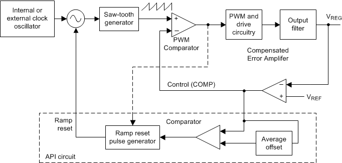
Figure 10 shows the control loop with API technology. The control scheme continuously senses the voltage on the COMP pin to determine a transient event that could require a sudden increase in duty-cycle. Upon detecting such an event, additional pulses are asynchronously injected in the PWM stream to quickly respond to the transient and arrest any undershoot in the output voltage.
Refer to the MFR_SPECIFIC_32 (API_OPTIONS) (F0h) section for more information.
The API response can be delayed by compensation, parasitic impedance between the output inductor and the voltage sense point. If the delay is large, the asynchronous PWM might inject too much energy and result in overshoot during load step-up. In this case, it is imperative to optimize the compensation and reduce the parasitic impedance. If these efforts cannot reduce the overshoot to an acceptable level, disable the API function.
 Figure 10. API Block Diagram