SLUSBO6C JANUARY 2014 – October 2018 TPS40425
PRODUCTION DATA.
- 1 Features
- 2 Applications
- 3 Description
- 4 Revision History
- 5 Pin Configuration and Functions
- 6 Specifications
-
7 Detailed Description
- 7.1 Overview
- 7.2 Functional Block Diagram
- 7.3
Feature Description
- 7.3.1 Asynchronous Pulse Injection (API)
- 7.3.2 Adaptive Voltage Scaling (AVS)
- 7.3.3 Switching Frequency and Synchronization
- 7.3.4 Voltage Reference
- 7.3.5 Output Voltage and Remote Sensing Amplifier
- 7.3.6 Current Sensing and Temperature Sensing Modes
- 7.3.7 Current Sensing
- 7.3.8 Temperature Sensing
- 7.3.9 Current Sharing
- 7.3.10 Linear Regulators
- 7.3.11 Power Sequence Between TPS40425 Device and Power Stage
- 7.3.12 PWM Signal
- 7.3.13 Startup and Shutdown
- 7.3.14 Pre-Biased Output Start-up
- 7.3.15 PGOOD Indication
- 7.3.16 Overcurrent Protection
- 7.3.17 Overvoltage/Undervoltage Protection
- 7.3.18 Overtemperature Fault Protection
- 7.3.19 Input Undervoltage Lockout (UVLO)
- 7.3.20 Fault Communication
- 7.3.21 Fault Protection Summary
- 7.4 Device Functional Modes
- 7.5 Programming
- 7.6 Register Maps
- 7.7
Supported PMBus Commands
- 7.7.1 PAGE (00h)
- 7.7.2 OPERATION (01h)
- 7.7.3 ON_OFF_CONFIG (02h)
- 7.7.4 CLEAR_FAULTS (03h)
- 7.7.5 WRITE_PROTECT (10h)
- 7.7.6 STORE_USER_ALL (15h)
- 7.7.7 RESTORE_USER_ALL (16h)
- 7.7.8 CAPABILITY (19h)
- 7.7.9 VOUT_MODE (20h)
- 7.7.10 VIN_ON (35h)
- 7.7.11 VIN_OFF (36h)
- 7.7.12 IOUT_CAL_GAIN (38h)
- 7.7.13 IOUT_CAL_OFFSET (39h)
- 7.7.14 IOUT_OC_FAULT_LIMIT (46h)
- 7.7.15 IOUT_OC_FAULT_RESPONSE (47h)
- 7.7.16 IOUT_OC_WARN_LIMIT (4Ah)
- 7.7.17 OT_FAULT_LIMIT (4Fh)
- 7.7.18 OT_WARN_LIMIT (51h)
- 7.7.19 TON_RISE (61h)
- 7.7.20 STATUS_BYTE (78h)
- 7.7.21 STATUS_WORD (79h)
- 7.7.22 STATUS_VOUT (7Ah)
- 7.7.23 STATUS_IOUT (7Bh)
- 7.7.24 STATUS_TEMPERATURE (7Dh)
- 7.7.25 STATUS_CML (7Eh)
- 7.7.26 STATUS_MFR_SPECIFIC (80h)
- 7.7.27 READ_VOUT (8Bh)
- 7.7.28 READ_IOUT (8Ch)
- 7.7.29 READ_TEMPERATURE_2 (8Eh)
- 7.7.30 PMBus_REVISION (98h)
- 7.7.31 MFR_SPECIFIC_00 (D0h)
- 7.7.32 MFR_SPECIFIC_04 (VREF_TRIM) (D4h)
- 7.7.33 MFR_SPECIFIC_05 (STEP_VREF_MARGIN_HIGH) (D5h)
- 7.7.34 MFR_SPECIFIC_06 (STEP_VREF_MARGIN_LOW) (D6h)
- 7.7.35 MFR_SPECIFIC_07 (PCT_VOUT_FAULT_PG_LIMIT) (D7h)
- 7.7.36 MFR_SPECIFIC_08 (SEQUENCE_TON_TOFF_DELAY) (D8h)
- 7.7.37 MFR_SPECIFIC_16 (COMM_EEPROM_SPARE) (E0h)
- 7.7.38 MFR_SPECIFIC_21 (OPTIONS) (E5h)
- 7.7.39 MFR_SPECIFIC_22 (PWM_OSC_SELECT) (E6h)
- 7.7.40 MFR_SPECIFIC_23 (MASK SMBALERT) (E7h)
- 7.7.41 MFR_SPECIFIC_25 (AVS_CONFIG) (E9h)
- 7.7.42 MFR_SPECIFIC_26 (AVS_ADDRESS) (EAh)
- 7.7.43 MFR_SPECIFIC_27 (AVS_DAC_DEFAULT) (EBh)
- 7.7.44 MFR_SPECIFIC_28 (AVS_CLAMP_HI) (ECh)
- 7.7.45 MFR_SPECIFIC_29 (AVS_CLAMP_LO) (EDh)
- 7.7.46 MFR_SPECIFIC_30 (TEMP_OFFSET) (EEh)
- 7.7.47 MFR_SPECIFIC_32 (API_OPTIONS) (F0h)
- 7.7.48 MFR_SPECIFIC_44 (DEVICE_CODE) (FCh)
-
8 Applications and Implementation
- 8.1 Application Information
- 8.2
Typical Application
- 8.2.1 Dual-Output Application
- 8.2.2 Design Requirements
- 8.2.3
Design Procedure
- 8.2.3.1 Switching Frequency Selection
- 8.2.3.2 Inductor Selection
- 8.2.3.3 Output Capacitor Selection
- 8.2.3.4 Input Capacitor Selection
- 8.2.3.5 VDD, BP5, BP3 Bypass Capacitor
- 8.2.3.6 R-C Snubber
- 8.2.3.7 Current and Temperature Sensor
- 8.2.3.8 Power Sequence Between the TPS40425 Device and Power Stage
- 8.2.3.9 Output Voltage Setting and Frequency Compensation Selection
- 8.2.3.10 Key PMBus Parameter Selection
- 8.2.4 Application Curves
- 9 Power Supply Recommendations
- 10Layout
- 11Device and Documentation Support
- 12Mechanical, Packaging, and Orderable Information
Package Options
Mechanical Data (Package|Pins)
- RHA|40
Thermal pad, mechanical data (Package|Pins)
- RHA|40
Orderable Information
7.3.7 Current Sensing
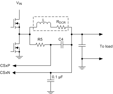
During non smart-power operation and while the controller uses inductor DCR for current sensing as shown in Figure 12, a filter must be used to remove the large AC component of voltage across the inductor and leave only the component of the voltage that appears across the resistance of the inductor. The values of R5 and C4 for the ideal case can be found using Equation 4. The time constant of the R-C filter should be equal to or greater than the time constant of the inductor. If the time constants are equal, the voltage appearing across C4 is the current in the inductor multiplied the inductor resistance. The voltage across C4 perfectly reflects the inductor ripple current in this case and there is no reason to have a shorter R-C time constant.
Extending the R-C filter time constant beyond the inductor time constant lowers the AC ripple component of voltage present at the current sense pins of the TPS40425 device but allows the correct DC current information to remain intact. This extension also delays slightly the response to an overcurrent event, but reduces noise in the system leading to cleaner overcurrent performance and current reporting data over the PMBus. The extension of R-C filter time slightly affects control loop during multi-phase operation, because the current information is applied to the loop to achieve current balance between the phases.
In all cases, C4 should be placed as close to current sense pins as possible to help avoid problems with noise and a decoupling capacitor connected to the CSxN pin is suggested.

where
- R5 and RDCR are in Ω
- C4 is in F (C4 is suggested to be larger than 220 nF)
- L is in H
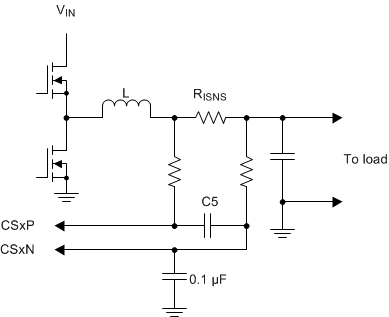
When a sensing resistor performs the current sensing, an R-C-R filter as shown in Figure 13 is recommended to filter noise.
 Figure 12. Current Sensing Using DCR
  Figure 13. Current Sensing Using Sense Resistor
 NOTE
The programming range of current sense element resistance is between 0.244 mΩ and 7.747 mΩ. The IOUT_CAL_GAIN command sets the value of the current sense element resistance. The maximum difference between CSP and CSN is limited to 60 mV by the current-sharing and current-limit circuit. However, under some conditions, the current-monitoring circuit has tighter limits, as follows:
- For sense element resistance between 0.244 mΩ and 0.5795 mΩ, the maximum differential voltage is 24 mV
- For sense element resistance between 0.5795 mΩ and 1.1285 mΩ, the maximum differential voltage is 40 mV
- For sense element resistance higher than 1.1285 mΩ, the maximum differential voltage is 60 mV
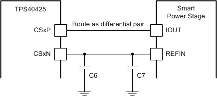
During smart-power operation current sense as Figure 14 shows, the design requires local bypass capacitors for the CSxN pin of the TPS40425 device and the REFIN pin of the smart power stage to avoid noise problems. The recommended value of C6 is 100 nF. Refer to the datasheet of the smart power stage for a C7 value. The two current signal traces must be routed as a differential pair on quiet area.
 Figure 14. Current Sensing using Smart-Power Stage
 NOTE
During smart-power mode operation, the IOUT_CAL_GAIN must be set to 0.5 mΩ.