SLUSEZ1A December   2023  – December 2024 TPS4800-Q1

PRODUCTION DATA  

  1.   1
  2. Features
  3. Applications
  4. Description
  5. Pin Configuration and Functions
  6. Specifications
    1. 5.1 Absolute Maximum Ratings
    2. 5.2 ESD Ratings
    3. 5.3 Recommended Operating Conditions
    4. 5.4 Thermal Information
    5. 5.5 Electrical Characteristics
    6. 5.6 Switching Characteristics
    7. 5.7 Typical Characteristics
  7. Parameter Measurement Information
  8. Detailed Description
    1. 7.1 Overview
    2. 7.2 Functional Block Diagram
    3. 7.3 Feature Description
      1. 7.3.1 Charge Pump and Gate Driver Output (VS, PU, PD, BST, SRC)
      2. 7.3.2 Capacitive Load Driving Using FET Gate (PU, PD) Slew Rate Control
      3. 7.3.3 Short-Circuit Protection
        1. 7.3.3.1 Short-Circuit Protection With Auto-Retry
        2. 7.3.3.2 Short-Circuit Protection With Latch-Off
      4. 7.3.4 Overvoltage (OV) and Undervoltage Protection (UVLO)
      5. 7.3.5 Reverse Polarity Protection
      6. 7.3.6 Short-Circuit Protection Diagnosis (SCP_TEST)
      7. 7.3.7 TPS48000-Q1 as a Simple Gate Driver
    4. 7.4 Device Functional Modes
  9. Application and Implementation
    1. 8.1 Application Information
    2. 8.2 Typical Application: Driving Power at all Times (PAAT) Loads
      1. 8.2.1 Design Requirements
      2. 8.2.2 Detailed Design Procedure
      3. 8.2.3 Application Curves
    3. 8.3 Power Supply Recommendations
    4. 8.4 Layout
      1. 8.4.1 Layout Guidelines
      2. 8.4.2 Layout Example
  10. Device and Documentation Support
    1. 9.1 Receiving Notification of Documentation Updates
    2. 9.2 Support Resources
    3. 9.3 Trademarks
    4. 9.4 Electrostatic Discharge Caution
    5. 9.5 Glossary
  11. 10Revision History
  12. 11Mechanical, Packaging, and Orderable Information

Package Options

Refer to the PDF data sheet for device specific package drawings

Mechanical Data (Package|Pins)
  • DGX|19
Thermal pad, mechanical data (Package|Pins)
Orderable Information

Typical Characteristics

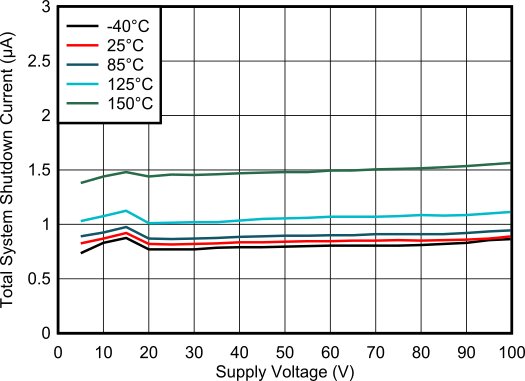
TPS4800-Q1 Shutdown Supply Current vs Supply Voltage
 
Figure 5-1 Shutdown Supply Current vs Supply Voltage
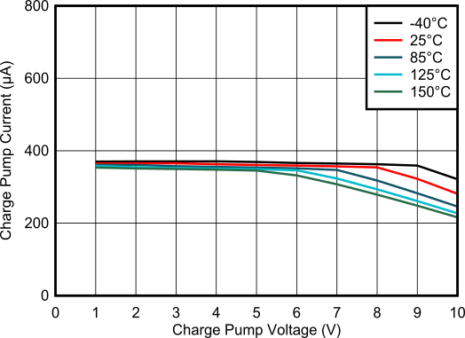
TPS4800-Q1 Charge Pump Current vs Charge Pump Voltage
 
Figure 5-3 Charge Pump Current vs Charge Pump Voltage
TPS4800-Q1 Charge Pump UVLO Thresholds vs Temperature
 
Figure 5-5 Charge Pump UVLO Thresholds vs Temperature
TPS4800-Q1 Short
                        Circuit Protection Response Time (tSC) vs Temperature
 
Figure 5-7 Short Circuit Protection Response Time (tSC) vs Temperature
TPS4800-Q1 Input
                        Supply UVLO Thresholds vs Temperature
 
Figure 5-9 Input Supply UVLO Thresholds vs Temperature
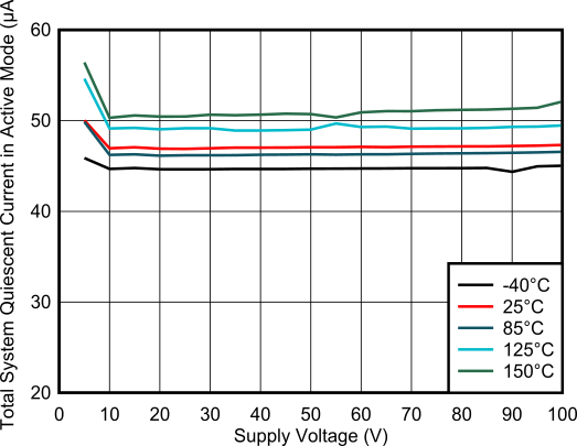
TPS4800-Q1 Operating Quiescent Current in Active Mode vs Supply Voltage
 
Figure 5-2 Operating Quiescent Current in Active Mode vs Supply Voltage
TPS4800-Q1 BST
                        Loading Current (I(BST)) vs Temperature
V(BST) = 15 V  V(SRC) = 0 V
Figure 5-4 BST Loading Current (I(BST)) vs Temperature
TPS4800-Q1 Short-Circuit Threshold (V(SCP)) vs Temperature
 
Figure 5-6 Short-Circuit Threshold (V(SCP)) vs Temperature
TPS4800-Q1 Input
                        Supply POR Thresholds vs Temperature
 
Figure 5-8 Input Supply POR Thresholds vs Temperature