SLUSEW1A January 2024 – December 2024 TPS4810-Q1
PRODUCTION DATA
- 1
- 1 Features
- 2 Applications
- 3 Description
- 4 Pin Configuration and Functions
- 5 Specifications
- 6 Parameter Measurement Information
-
7 Detailed Description
- 7.1 Overview
- 7.2 Functional Block Diagram
- 7.3
Feature Description
- 7.3.1 Charge Pump and Gate Driver Output (VS, G1PU, G1PD, G2, BST, SRC)
- 7.3.2 Capacitive Load Driving Using FET Gate (G1PU, G1PD) Slew Rate Control
- 7.3.3 Short-Circuit Protection
- 7.3.4 Undervoltage Protection (UVLO)
- 7.3.5 Reverse Polarity Protection
- 7.3.6 Short-Circuit Protection Diagnosis (SCP_TEST)
- 7.3.7 TPS48100-Q1 as a Simple Gate Driver
- 7.4 Device Functional Modes
- 8 Application and Implementation
- 9 Device and Documentation Support
- 10Revision History
- 11Mechanical, Packaging, and Orderable Information
Package Options
Mechanical Data (Package|Pins)
- DGX|19
Thermal pad, mechanical data (Package|Pins)
Orderable Information
8.2.3 Application Curves
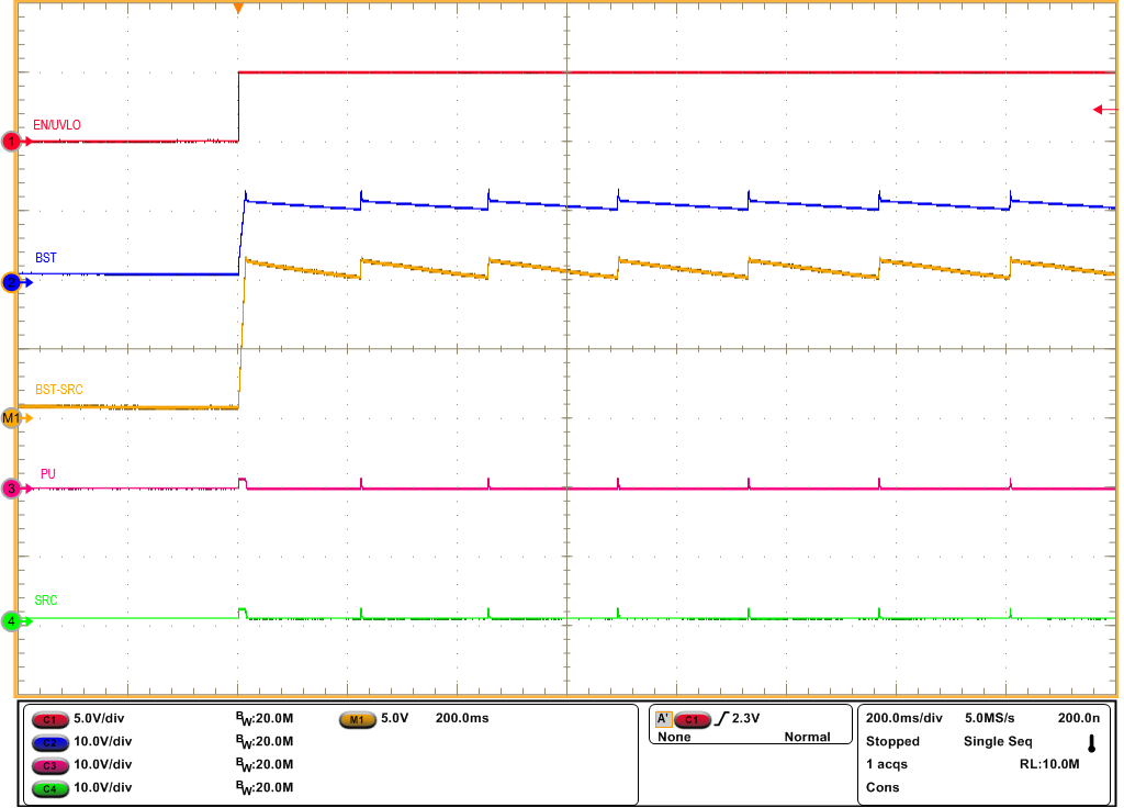 Figure 8-2 Start-Up Profile of Bootstrap Voltage With
INP1 = INP2 = GND and CBST = 470nF
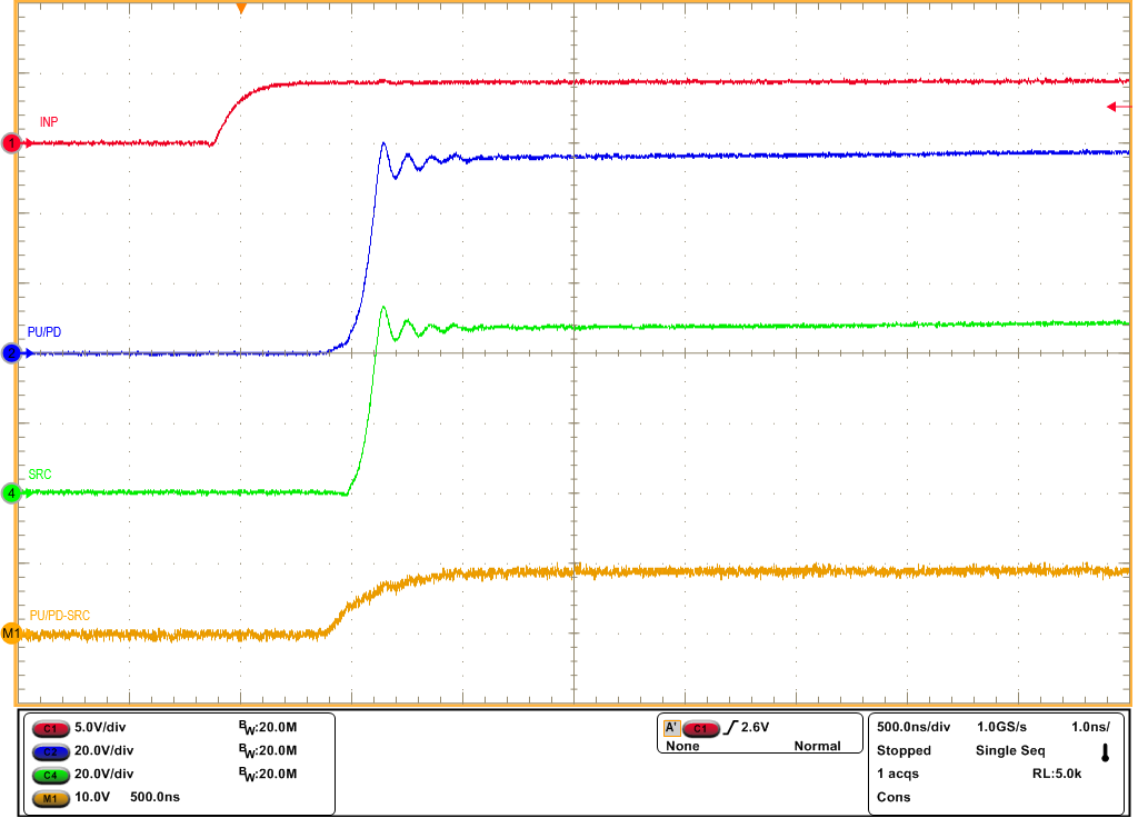 Figure 8-4 Turn-ON Response of TPS48100-Q1 for INP1 ->
LOW to HIGH and CBST = 470nF
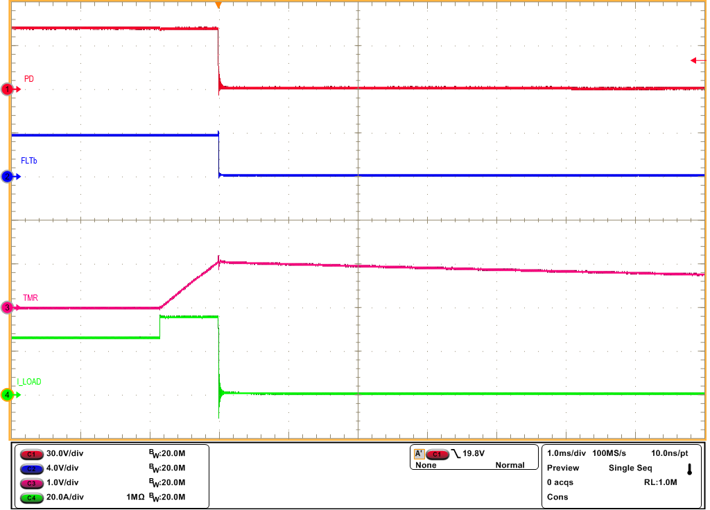 Figure 8-6 Overcurrent Response of TPS48100-Q1 for a Load
Step From 25A to 35A With 30A Overcurrent Protection Setting
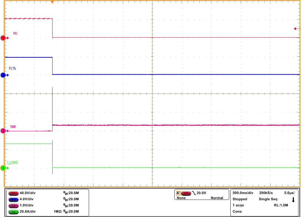 Figure 8-8 Latch-Off Response of TPS48100-Q1 for an Overcurrent Fault
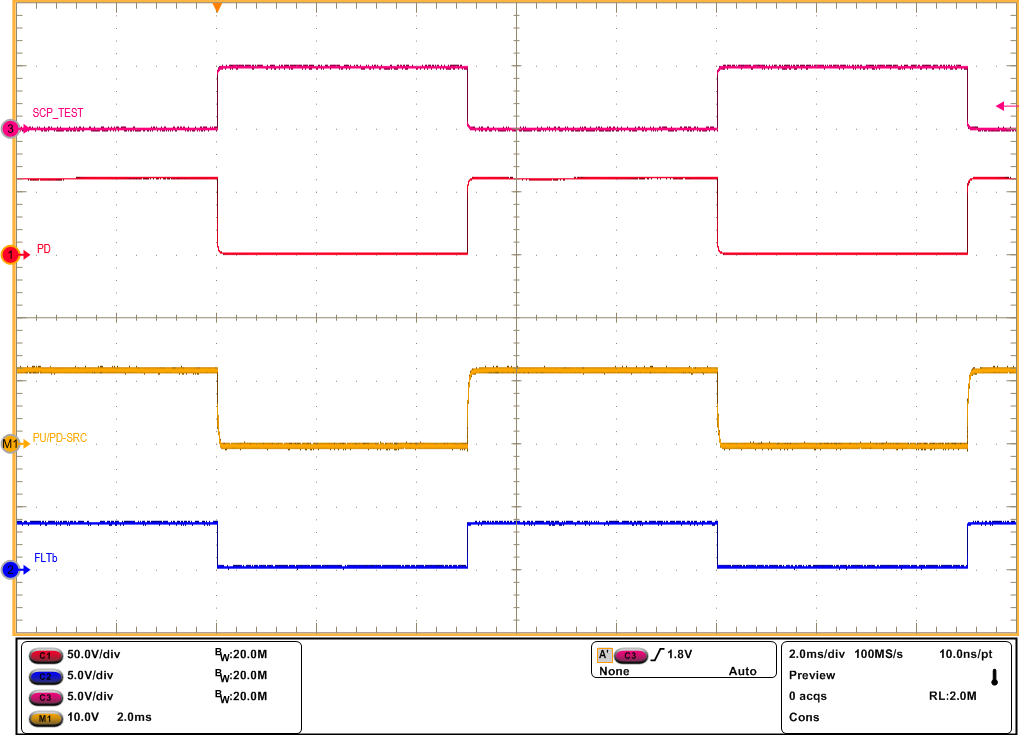 Figure 8-10 Short-Circuit Protection Diagnosis Test Response of TPS48100-Q1
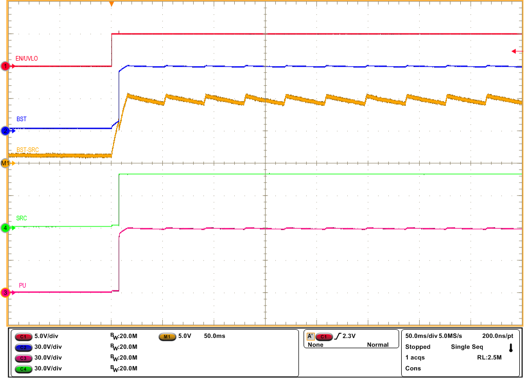 Figure 8-3 Start-Up Profile of Bootstrap Voltage With INP1 = INP2 = HIGH and CBST =
470nF
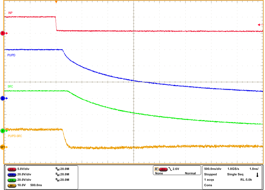 Figure 8-5 Turn-OFF Response of TPS48100-Q1 for INP1
-> HIGH to LOW and CBST = 470nF
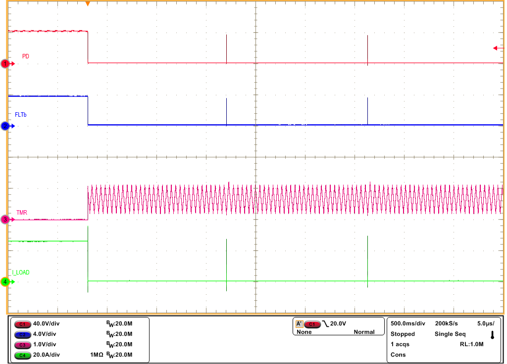 Figure 8-7 Auto-Retry Response of TPS48100-Q1 for an Overcurrent Fault
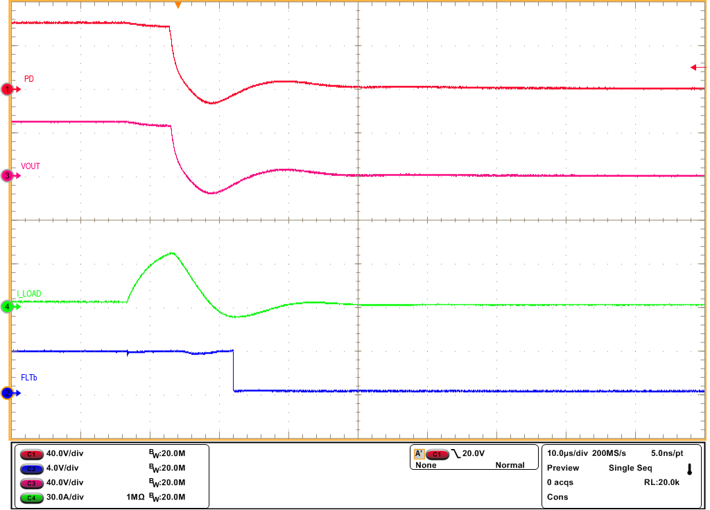 Figure 8-9 Output Short-Circuit Response of TPS48100-Q1 Device