SLVSD73B
December 2015 – March 2018
TPS4H000-Q1
PRODUCTION DATA.
1
Features
2
Applications
3
Description
Device Images
Typical Application Schematic
Driving a Capacitive Load With Adjustable Current Limit
4
Revision History
5
Device Comparison Table
6
Pin Configuration and Functions
Pin Functions
7
Specifications
7.1
Absolute Maximum Ratings
7.2
ESD Ratings
7.3
Recommended Operating Conditions
7.4
Thermal Information
7.5
Electrical Characteristics
7.6
Switching Characteristics
7.7
Typical Characteristics
8
Detailed Description
8.1
Overview
8.2
Functional Block Diagram
8.3
Feature Description
8.3.1
Pin Current and Voltage Conventions
8.3.2
Accurate Current Sense
8.3.3
Adjustable Current Limit
8.3.4
Inductive-Load Switching-Off Clamp
8.3.5
Fault Detection and Reporting
8.3.5.1
Diagnostic Enable Function
8.3.5.2
Multiplexing of Current Sense
8.3.5.3
Fault Table
8.3.5.4
STx and FAULT Reporting
8.3.6
Full Diagnostics
8.3.6.1
Short-to-GND and Overload Detection
8.3.6.2
Open-Load Detection
8.3.6.2.1
Channel On
8.3.6.2.2
Channel Off
8.3.6.3
Short-to-Battery Detection
8.3.6.4
Reverse Polarity Detection
8.3.6.5
Thermal Fault Detection
8.3.6.5.1
Thermal Shutdown
8.3.7
Full Protections
8.3.7.1
UVLO Protection
8.3.7.2
Loss-of-GND Protection
8.3.7.3
Protection for Loss of Power Supply
8.3.7.4
Reverse-Current Protection
8.3.7.5
MCU I/O Protection
8.4
Device Functional Modes
8.4.1
Working Modes
9
Application and Implementation
9.1
Application Information
9.2
Typical Application
9.2.1
Design Requirements
9.2.2
Detailed Design Procedure
9.2.3
Application Curves
10
Power Supply Recommendations
11
Layout
11.1
Layout Guidelines
11.2
Layout Examples
11.2.1
Without a GND Network
11.2.2
With a GND Network
12
Device and Documentation Support
12.1
Receiving Notification of Documentation Updates
12.2
Community Resources
12.3
Trademarks
12.4
Electrostatic Discharge Caution
12.5
Glossary
13
Mechanical, Packaging, and Orderable Information
Package Options
Mechanical Data (Package|Pins)
PWP|20
MHTS001G
Thermal pad, mechanical data (Package|Pins)
PWP|20
PPTD027Z
Orderable Information
slvsd73b_oa
slvsd73b_pm
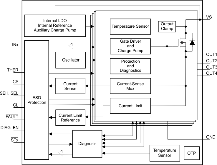
8.2
Functional Block Diagram