SLVSD73B December 2015 – March 2018 TPS4H000-Q1
PRODUCTION DATA.
- 1 Features
- 2 Applications
- 3 Description
- 4 Revision History
- 5 Device Comparison Table
- 6 Pin Configuration and Functions
- 7 Specifications
-
8 Detailed Description
- 8.1 Overview
- 8.2 Functional Block Diagram
- 8.3 Feature Description
- 8.4 Device Functional Modes
- 9 Application and Implementation
- 10Power Supply Recommendations
- 11Layout
- 12Device and Documentation Support
- 13Mechanical, Packaging, and Orderable Information
Package Options
Mechanical Data (Package|Pins)
- PWP|20
Thermal pad, mechanical data (Package|Pins)
- PWP|20
Orderable Information
8.3.6.5.1 Thermal Shutdown
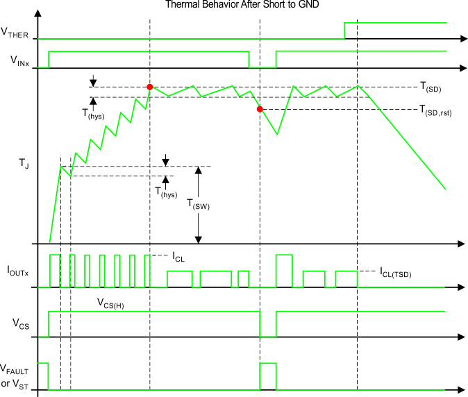
Thermal shutdown is active when the absolute temperature TJ> T(SD). When thermal shutdown occurs, the respective output turns off. The THER pin is used to configure the behavior after the thermal shutdown occurs.
- When the THER pin is low, thermal shutdown operates in the auto-retry mode. The output automatically recovers when TJ< T(SD) – T(hys), but the current is limited to ICL(TSD) to avoid repetitive thermal shutdown. The thermal shutdown fault signal is cleared when TJ< T(SD,rst) or after toggling the related INx pin.
- When the THER pin is high, thermal shutdown operates in the latch mode. The output latches off when thermal shutdown occurs. When the THER pin goes from high to low, thermal shutdown changes to auto-retry mode. The thermal shutdown fault signal is cleared after toggling the related INx pin.
Thermal swing activates when the power FET temperature is increasing sharply, that is, when ΔT = T(FET) – T(Logic)> T(sw), then the output turns off. The output automatically recovers and the fault signal clears when ΔT = T(FET) – T(Logic)< T(sw) – T(hys). Thermal swing function improves the device reliability when subjected to repetitive fast thermal variation. As shown in Figure 31, multiple thermal swings are triggered before thermal shutdown occurs.
 Figure 31. Thermal Behavior Diagram