SLVSH18 December 2024 TPS4HC120-Q1
PRODUCTION DATA
- 1
- 1 Features
- 2 Applications
- 3 Description
- 4 Pin Configuration and Functions
- 5 Specifications
-
6 Detailed Description
- 6.1 Overview
- 6.2 Functional Block Diagram
- 6.3 Feature Description
- 6.4 Device Functional Modes
- 7 Application and Implementation
- 8 Device and Documentation Support
- 9 Revision History
- 10Mechanical, Packaging, and Orderable Information
Package Options
Mechanical Data (Package|Pins)
- DGQ|28
Thermal pad, mechanical data (Package|Pins)
Orderable Information
6.3.5 Inductive-Load Switching-Off Clamp
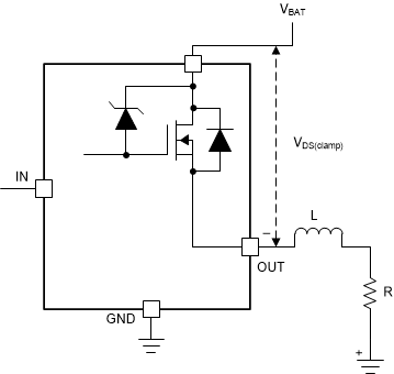
When switching an inductive load off, the inductive reactance tends to pull the output voltage negative. Excessive negative voltage could cause the power FET to break down. To protect the power FET, an internal clamp between drain and source is implemented, namely VDS(clamp).

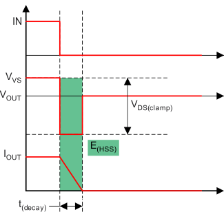
During the period of demagnetization (tdecay), the power FET is turned on for inductance-energy dissipation. The total energy is dissipated in the high-side switch. Total energy includes the energy of the power supply (E(VS)) and the energy of the load (E(load)). If resistance is in series with inductance, some of the load energy is dissipated on the resistance.

When an inductive load switches off, E(HSS) causes high thermal stressing on the device. The upper limit of the power dissipation depends on the device intrinsic capacity, ambient temperature, and board dissipation condition.
 Figure 6-10 Drain-to-Source Clamping Structure
 Figure 6-11 Inductive Load Switching-Off Diagram
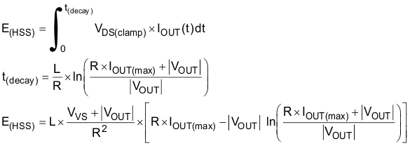
From the perspective of the high-side switch, E(HSS) equals the integration value during the demagnetization period.

When R approximately equals 0, E(HSD) can be given simply as:

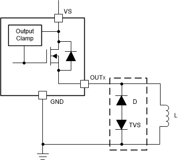
Note that for PWM-controlled inductive loads, it is recommended to add the external freewheeling circuitry shown in Figure 6-12 to protect the device from repetitive power stressing. TVS is used to achieve the fast decay. See Figure 6-12 for more details.
 Figure 6-12 Protection With External Circuitry