SLUS786H OCTOBER 2007 – January 2015 TPS51125
PRODUCTION DATA.
- 1 Features
- 2 Applications
- 3 Description
- 4 Revision History
- 5 Pin Configuration and Functions
- 6 Specifications
-
7 Detailed Description
- 7.1 Overview
- 7.2 Functional Block Diagram
- 7.3
Feature Description
- 7.3.1 PWM Operations
- 7.3.2 Adaptive On-Time Control and PWM Frequency
- 7.3.3 Loop Compensation
- 7.3.4 Ramp Signal
- 7.3.5 Light-Load Condition in Auto-Skip Operation
- 7.3.6 Out-of-Audio Light-Load Operation
- 7.3.7 VREG5/VREG3 Linear Regulators
- 7.3.8 VREG5 Switch Over
- 7.3.9 VREG3 Switch Over
- 7.3.10 Powergood
- 7.3.11 Output Discharge Control
- 7.3.12 Low-Side Driver
- 7.3.13 High-Side Driver
- 7.3.14 VCLK for Charge Pump
- 7.3.15 Current Protection
- 7.3.16 Overvoltage and Undervoltage Protection
- 7.3.17 UVLO Protection
- 7.3.18 Thermal Shutdown
- 7.4 Device Functional Modes
- 8 Application and Implementation
- 9 Power Supply Recommendations
- 10Layout
- 11Device and Documentation Support
- 12Mechanical, Packaging, and Orderable Information
Package Options
Mechanical Data (Package|Pins)
- RGE|24
Thermal pad, mechanical data (Package|Pins)
- RGE|24
Orderable Information
8 Application and Implementation
NOTE
Information in the following applications sections is not part of the TI component specification, and TI does not warrant its accuracy or completeness. TI’s customers are responsible for determining suitability of components for their purposes. Customers should validate and test their design implementation to confirm system functionality.
8.1 Application Information
The TPS51125 is typically used as a dual-synchronous buck controller, which convert an input voltage ranging from 5.5 V to 28 V, to output voltage 5 V and 3.3 V respectively, targeted for notebook system-power supply solutions.
8.2 Typical Application
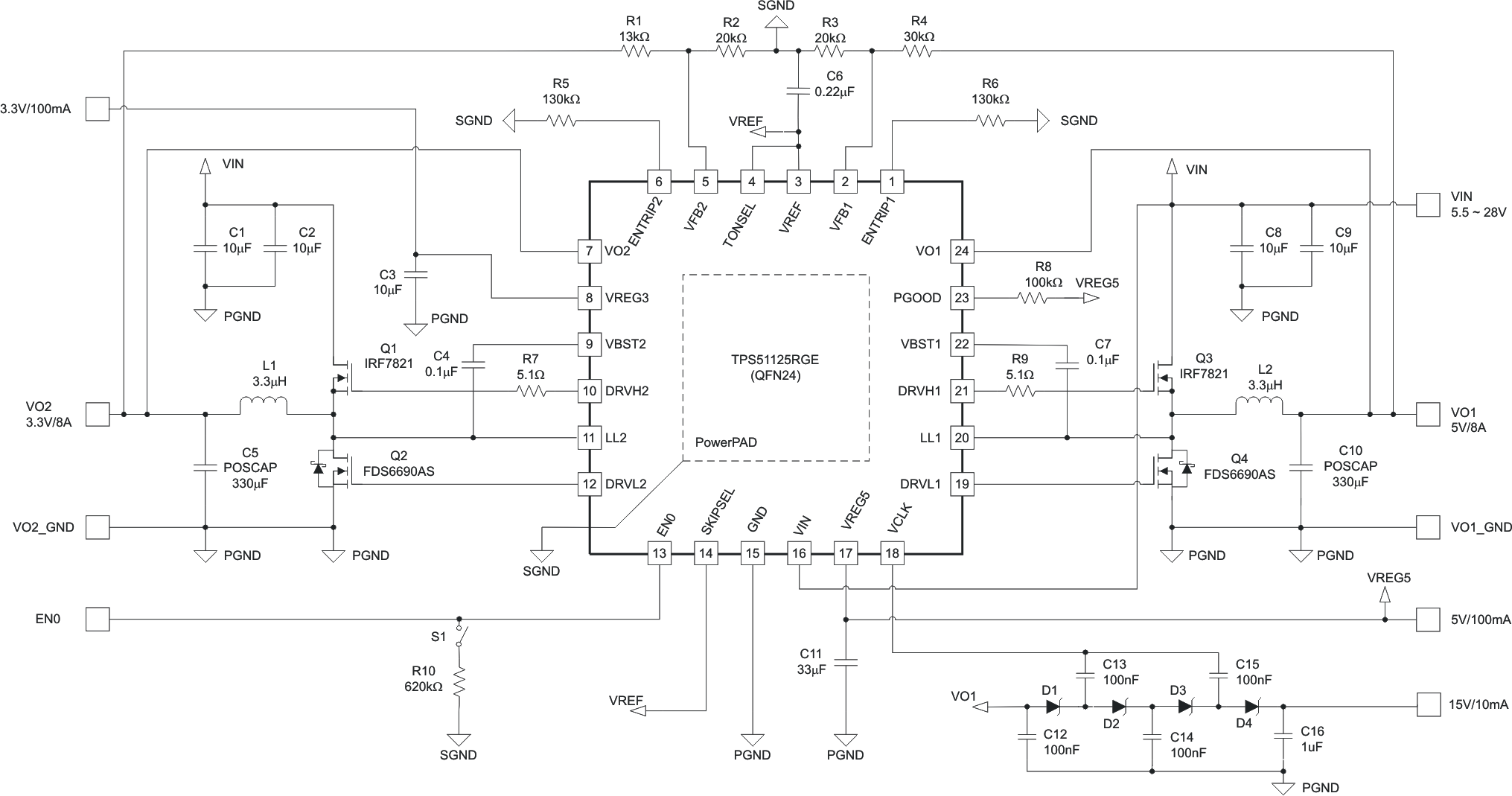 Figure 34. 5-V/8-A, 3.3-V/8-A Application Circuit (245-kHz/305-kHz Setting)
8.2.1 Design Requirements
Table 3. Design Parameters
| PARAMETER | VALUE | ||
|---|---|---|---|
| Input voltage range | 5.5 V to 28 V | ||
| Channel 1 output voltage | 5 V | ||
| Channel 1 output current | 8 A | ||
| Channel 2 output voltage | 3.3 V | ||
| Channel 2 output current | 8 A |
8.2.2 Detailed Design Procedure
Table 4. List of Materials for 5-V / 8-A, 3.3-V / 8-A Application Circuit
| SYMBOL | SPECIFICATION | MANUFACTURER | PART NUMBER |
|---|---|---|---|
| C1, C2, C8, C9 | 10 μ F, 25 V | Taiyo Yuden | TMK325BJ106MM |
| C3 | 10 μF, 6.3 V | TDK | C2012X5R0J106K |
| C11 | 33 μF, 6.3 V | TDK | C3216X5RBJ336M |
| C5, C10 | 330 μF, 6.3 V, 25 mΩ | Sanyo | 6TPE330ML |
| L1, L2 | 3.3 μH, 15.6 A, 5.92 mΩ | TOKO | FDA1055-3R3M |
| Q1, Q3 | 30 V, 9.5 mΩ | IR | IRF7821 |
| Q2, Q4(1) | 30 V, 12 mΩ | Fairchild | FDS6690AS |
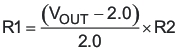
8.2.2.1 Determine Output Voltage
The output voltage is programmed by the voltage-divider resistor, R1 and R2 shown in Figure 31. R1 is connected between VFBx pin and the output, and R2 is connected betwen the VFBx pin and GND. Recommended R2 value is from 10 kΩ to 20 kΩ. Determine R1 using equation as below.
8.2.2.2 Choose the Inductor
The inductance value should be determined to give the ripple current of approximately 1/4 to 1/2 of maximum output current. Larger ripple current increases output ripple voltage and improves S/N ratio and helps stable operation.
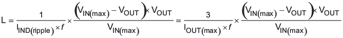
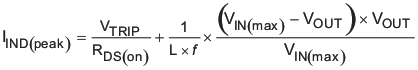
The inductor also needs to have low DCR to achieve good efficiency, as well as enough room above peak inductor current before saturation. The peak inductor current can be estimated as follows.
8.2.2.3 Choose the Output Capacitors
Organic semiconductor capacitors or specialty polymer capacitors are recommended. Determine ESR to meet required ripple voltage. A quick approximation is as shown in Equation 8.
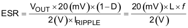
where
- D is the duty cycle
- the required output ripple slope is approximately 20 mV per tSW (switching period) in terms of VFB terminal voltage
8.2.2.4 Choose the Low-Side MOSFET
It is highly recommended that the low-side MOSFET should have an integrated Schottky barrier diode, or an external Schottky barrier diode in parallel to achieve stable operation.
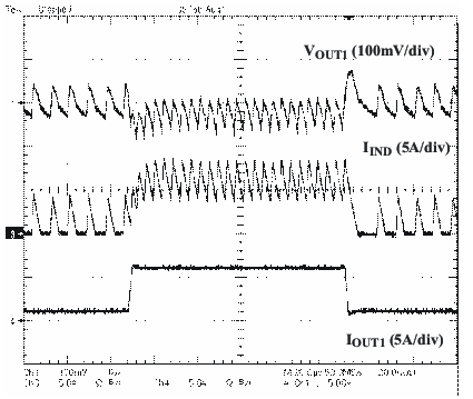
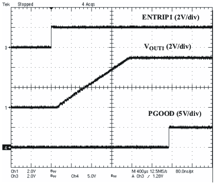
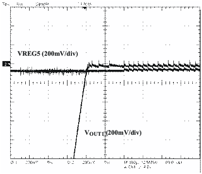
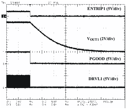
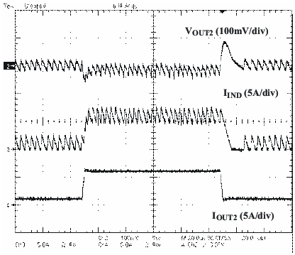
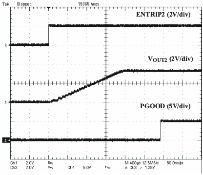
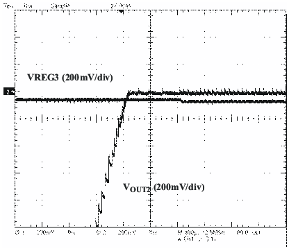
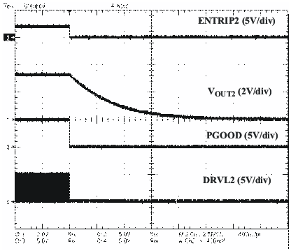
8.2.3 Application Curves