SLUS984C November   2009  – April 2018 TPS51200-Q1

PRODUCTION DATA.  

  1. Features
  2. Applications
  3. Description
    1.     Device Images
      1.      Standard DDR Application
  4. Revision History
  5. Pin Configuration and Functions
    1.     Pin Functions
  6. Specifications
    1. 6.1 Absolute Maximum Ratings
    2. 6.2 ESD Ratings
    3. 6.3 Recommended Operating Conditions
    4. 6.4 Thermal Information
    5. 6.5 Electrical Characteristics
    6. 6.6 Switching Characteristics
    7. 6.7 Typical Characteristics
  7. Detailed Description
    1. 7.1 Overview
    2. 7.2 Functional Block Diagram
    3. 7.3 Feature Description
      1. 7.3.1 Sink and Source Regulator (VO Pin)
      2. 7.3.2 Reference Input (REFIN Pin)
      3. 7.3.3 Reference Output (REFOUT Pin)
      4. 7.3.4 Soft-Start Sequencing
      5. 7.3.5 Enable Control (EN Pin)
      6. 7.3.6 Powergood Function (PGOOD Pin)
      7. 7.3.7 Current Protection (VO Pin)
      8. 7.3.8 UVLO Protection (VIN Pin)
      9. 7.3.9 Thermal Shutdown
    4. 7.4 Device Functional Modes
      1. 7.4.1 S3 and Pseudo-S5 Support
      2. 7.4.2 Tracking Startup and Shutdown
  8. Application and Implementation
    1. 8.1 Application Information
    2. 8.2 Typical Application
      1. 8.2.1 VTT DIMM Applications
        1. 8.2.1.1 Design Parameters
        2. 8.2.1.2 Detailed Design Procedure
          1. 8.2.1.2.1 VIN Capacitor
          2. 8.2.1.2.2 VLDO Input Capacitor
          3. 8.2.1.2.3 Output Capacitor
          4. 8.2.1.2.4 Output Tolerance Consideration for VTT DIMM Applications
        3. 8.2.1.3 Application Curves
      2. 8.2.2 Design Example 1
        1. 8.2.2.1 Design Parameters
      3. 8.2.3 Design Example 2
        1. 8.2.3.1 Design Parameters
      4. 8.2.4 Design Example 3
        1. 8.2.4.1 Design Parameters
      5. 8.2.5 Design Example 4
        1. 8.2.5.1 Design Parameters
      6. 8.2.6 Design Example 5
        1. 8.2.6.1 Design Parameters
      7. 8.2.7 Design Example 6
        1. 8.2.7.1 Design Parameters
      8. 8.2.8 Design Example 7
        1. 8.2.8.1 Design Parameters
  9. Power Supply Recommendations
  10. 10Layout
    1. 10.1 Layout Guidelines
    2. 10.2 Layout Example
    3. 10.3 Thermal Considerations
  11. 11Device and Documentation Support
    1. 11.1 Device Support
      1. 11.1.1 Third-Party Products Disclaimer
    2. 11.2 Documentation Support
      1. 11.2.1 Related Documentation
    3. 11.3 Receiving Notification of Documentation Updates
    4. 11.4 Community Resource
    5. 11.5 Trademarks
    6. 11.6 Electrostatic Discharge Caution
    7. 11.7 Glossary
  12. 12Mechanical, Packaging, and Orderable Information

Package Options

Mechanical Data (Package|Pins)
Thermal pad, mechanical data (Package|Pins)
Orderable Information

VTT DIMM Applications

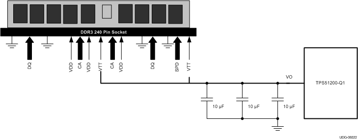
TPS51200-Q1 v08022_slus984.gifFigure 21. Typical Application Diagram for DDR3 VTT DIMM using TPS51200-Q1