SLUSDW9A June 2020 – June 2020 TPS51215A
PRODUCTION DATA.
- 1 Features
- 2 Applications
- 3 Description
- 4 Revision History
- 5 Pin Configuration and Functions
- 6 Specifications
-
7 Detailed Description
- 7.1 Overview
- 7.2 Functional Block Diagram
- 7.3
Feature Description
- 7.3.1 Switch Mode Power Supply Control
- 7.3.2 VREF, V0, V1, V2, V3 and Output Voltage
- 7.3.3 Soft-Start and Power Good
- 7.3.4 SLEW and VID Function
- 7.3.5 MODE Pin Configuration
- 7.3.6 Light-Load Operation
- 7.3.7 Out-of-Bound Operation
- 7.3.8 Current Sensing and Overcurrent Protection
- 7.3.9 Overvoltage and Undervoltage Protection
- 7.3.10 V5IN Undervoltage Lockout Protection
- 7.3.11 Thermal Shutdown
- 7.4 D-CAP2 Control Mode
- 8 Application and Implementation
-
9 Typical Applications
- 9.1 Design Requirements
- 9.2
Detailed Design Procedure
- 9.2.1 Step One: Determine the Specifications
- 9.2.2 Step Two: Determine System Parameters
- 9.2.3 Step Three: Determine Inductor Value and Choose Inductor
- 9.2.4 Step Four: Set the Output Voltages
- 9.2.5 Step Five: Calculate SLEW Capacitance
- 9.2.6 Step Six
- 9.2.7 Step Seven: Determine the Output Capacitance
- 9.2.8 Step Eight: Select Decoupling and Peripheral Components
- 9.3 Application Examples
- 9.4 Application Curves of Design 1
- 10Power Supply Recommendations
- 11Layout
- 12Device and Documentation Support
- 13Mechanical, Packaging, and Orderable Information
Package Options
Mechanical Data (Package|Pins)
- RUK|20
Thermal pad, mechanical data (Package|Pins)
- RUK|20
Orderable Information
11.1 Layout Guidelines
Certain issues must be considered before designing a layout using the TPS51215A.
- VIN capacitor(s), VOUT capacitor(s) and MOSFETs are the power components and should be placed on one side of the PCB (solder side). Other small signal components should be placed on another side (component side). At least one inner plane should be inserted, connected to ground, in order to shield and isolate the small signal traces from noisy power lines.
- All sensitive analog traces and components such as VSNS, SLEW, MODE, V0, V1, V2, V3, VREF and TRIP should be placed away from high-voltage switching nodes such as SW, DH, DL or BST to avoid coupling. Use internal layer(s) as ground plane(s) and shield feedback trace from power traces and components. Need to placed close to the part and minimized length of routing trace.
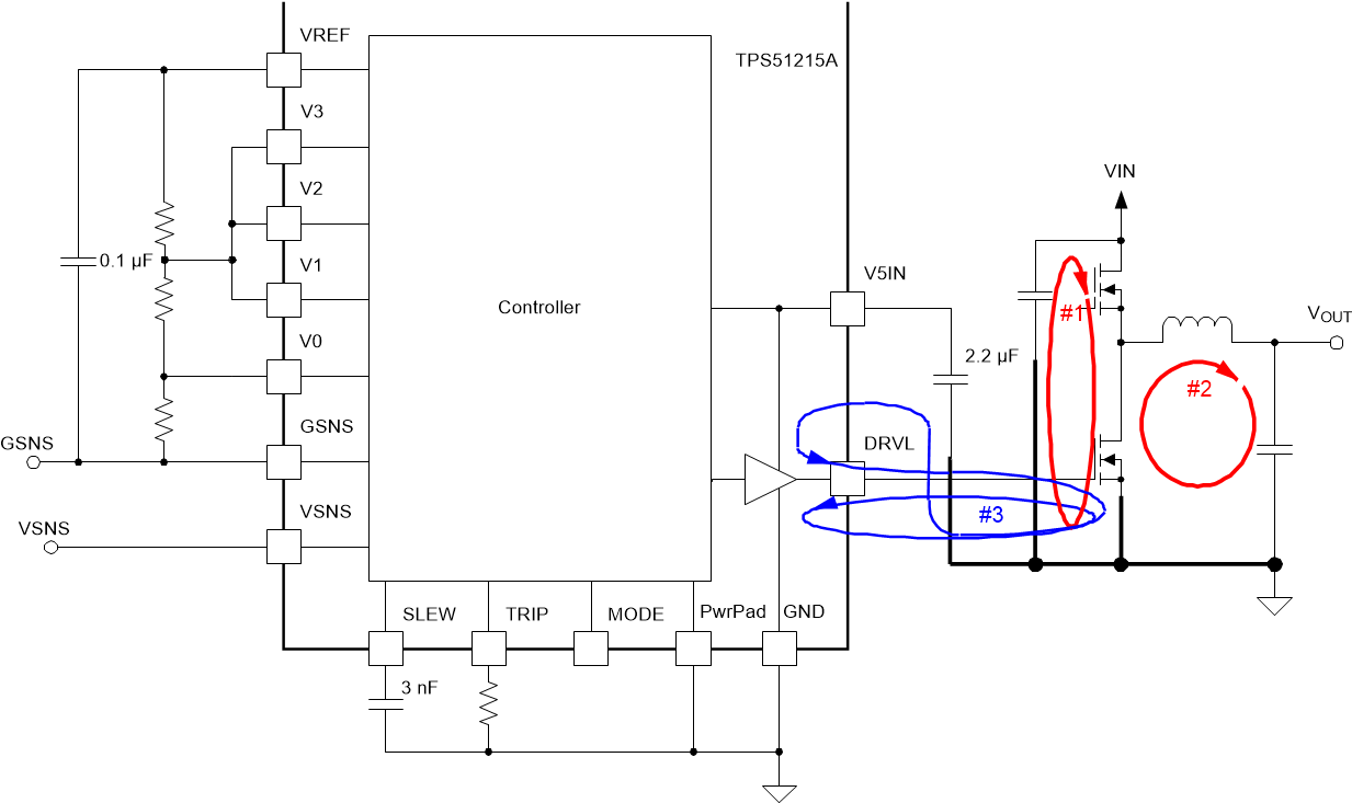
- The DC/DC converter has several high-current loops. The area of these loops should be minimized in order to suppress generating switching noise.
- Loop #1. The most important loop to minimize the area of is the path from the VIN capacitor(s) through the high and low-side MOSFETs, and back to the capacitor(s) through ground. Connect the negative node of the VIN capacitor(s) and the source of the low-side MOSFET at ground as close as possible. (Refer to loop #1 of Figure 26)
- Loop #2. The second important loop is the path from the low-side MOSFET through inductor and VOUT capacitor(s), and back to source of the low-side MOSFET through ground. Connect source of the low-side MOSFET and negative node of VOUT capacitor(s) at ground as close as possible. (Refer to loop #2 of Figure 26)
- Loop #3. The third important loop is of gate driving system for the low-side MOSFET. To turn on the low-side MOSFET, high current flows from V5 capacitor through gate driver and the low-side MOSFET, and back to negative node of the capacitor through ground. To turn off the low-side MOSFET, high current flows from gate of the low-side MOSFET through the gate driver and PGND, and back to source of the low-side MOSFET through ground. Connect negative node of V5 capacitor, source of the low-side MOSFET and PGND at ground as close as possible. (Refer to loop #3 of Figure 26)
- VSNS can be connected directly to the output voltage sense point at the load device or the bulk capacitor at the converter side. For additional noise filtering, insert a 10-Ω, 1-nF, R-C filter between the sense point and the VSNS pin. Connect GSNS to ground return point at the load device or the general ground plane/layer. VSNS and GSNS can be used for the purpose of remote sensing across the load device, however, care must be taken to minimize the routing trace to prevent excess noise injection to the sense lines.
- Connect the overcurrent setting resistors from TRIP pin to ground and make the connections as close as possible to the device. The trace from TRIP pin to resistor and from resistor to ground should avoid coupling to a high-voltage switching node.
- Connections from gate drivers to the respective gate of the high-side or the low-side MOSFET should be as short as possible to reduce stray inductance. Use 0.65 mm (25 mils) or wider trace and via(s) of at least 0.5 mm (20 mils) diameter along this trace.
- The PCB trace defined as SW node, which connects to the source of the switching MOSFET, the drain of the rectifying MOSFET and the high-voltage side of the inductor, should be as short and wide as possible.
- In order to effectively remove heat from the package, prepare the thermal land and solder to the package thermal pad. Wide trace of the component-side copper, connected to this thermal land, helps to dissipate heat Numerous vias with a 0.3-mm diameter connected from the thermal land to the internal/solder-side ground plane(s) should be used to help dissipation.
 Figure 26. DC/DC Converter Ground System