SLUSDW9A June 2020 – June 2020 TPS51215A
PRODUCTION DATA.
- 1 Features
- 2 Applications
- 3 Description
- 4 Revision History
- 5 Pin Configuration and Functions
- 6 Specifications
-
7 Detailed Description
- 7.1 Overview
- 7.2 Functional Block Diagram
- 7.3
Feature Description
- 7.3.1 Switch Mode Power Supply Control
- 7.3.2 VREF, V0, V1, V2, V3 and Output Voltage
- 7.3.3 Soft-Start and Power Good
- 7.3.4 SLEW and VID Function
- 7.3.5 MODE Pin Configuration
- 7.3.6 Light-Load Operation
- 7.3.7 Out-of-Bound Operation
- 7.3.8 Current Sensing and Overcurrent Protection
- 7.3.9 Overvoltage and Undervoltage Protection
- 7.3.10 V5IN Undervoltage Lockout Protection
- 7.3.11 Thermal Shutdown
- 7.4 D-CAP2 Control Mode
- 8 Application and Implementation
-
9 Typical Applications
- 9.1 Design Requirements
- 9.2
Detailed Design Procedure
- 9.2.1 Step One: Determine the Specifications
- 9.2.2 Step Two: Determine System Parameters
- 9.2.3 Step Three: Determine Inductor Value and Choose Inductor
- 9.2.4 Step Four: Set the Output Voltages
- 9.2.5 Step Five: Calculate SLEW Capacitance
- 9.2.6 Step Six
- 9.2.7 Step Seven: Determine the Output Capacitance
- 9.2.8 Step Eight: Select Decoupling and Peripheral Components
- 9.3 Application Examples
- 9.4 Application Curves of Design 1
- 10Power Supply Recommendations
- 11Layout
- 12Device and Documentation Support
- 13Mechanical, Packaging, and Orderable Information
Package Options
Mechanical Data (Package|Pins)
- RUK|20
Thermal pad, mechanical data (Package|Pins)
- RUK|20
Orderable Information
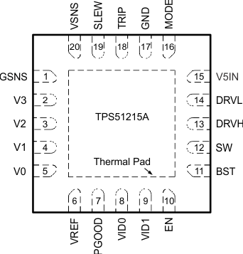
5 Pin Configuration and Functions
RUK Package
20-Pin WQFN
Top View

Pin Functions
| PIN | I/O | DESCRIPTION | |
|---|---|---|---|
| NAME | NO. | ||
| BST | 11 | I | Supply input for high-side MOSFET driver (bootstrap terminal). Connect a capacitor from this pin to the SW pin. Internally connected to V5IN via the bootstrap MOSFET switch. |
| DRVH | 13 | O | High-side MOSFET gate driver output. |
| DRVL | 14 | O | Synchronous low-side MOSFET gate driver output. |
| EN | 10 | I | Enable input for the device. Support 3.3-V logic |
| GND | 17 | I | Combined AGND and PGND point. The positive on-resistance current sensing input. |
| GSNS | 1 | I | Voltage sense return tied directly to GND sense point of the load. Tie to GND with a 10-Ω resistor to close feedback if remote sensing is used. Short to GND if remote sense is not used. |
| MODE | 16 | I | connect to V5IN |
| PGOOD | 7 | O | PGOOD output. Connect pull-up resistor. |
| SLEW | 19 | I | Program the startup using 4.5 µA and voltage transition time using 45 µA from an external capacitor via current source. |
| SW | 12 | I/O | High-side MOSFET gate driver return. The RDS(on) current sensing input (–). |
| TRIP | 18 | I | Connect resistor to GND to set OCL at VTRIP/8. Output 10 µA current at room temperature, TC = 4700ppm/°C. |
| V0 | 5 | I | Voltage need to be set to 0V, corresponding to 00 |
| V1 | 4 | I | Voltage set-point programming resistor input, corresponding to 01 |
| V2 | 3 | I | Voltage set-point programming resistor input, corresponding to 10 |
| V3 | 2 | I | Voltage set-point programming resistor input, corresponding to 11 |
| V5IN | 15 | I | 5-V power supply input for internal circuits and MOSFET gate drivers |
| VID0 | 8 | I | Logic input for set-point voltage selector. Use in conjunction with VID1 pin to select among four set-point reference voltages. Support 1-V and 3.3-V logic. |
| VID1 | 9 | I | Logic input for set-point voltage selector. Use in conjunction with VID0 pin to select among four set-point reference voltages. Support 1-V and 3.3-V logic. |
| VREF | 6 | O | 2 V, 300-µA voltage reference. Bypass to GND with a 1-µF ceramic capacitor. |
| VSNS | 20 | I | Voltage sense return tied directly to the load voltage sense point. Tie to VOUT with a 10-Ω resistor to close feedback if remote sensing is used. |
| Thermal Pad | — | — | Connect directly to system GND plane with multiple vias. |