SLUSDW9A June 2020 – June 2020 TPS51215A
PRODUCTION DATA.
- 1 Features
- 2 Applications
- 3 Description
- 4 Revision History
- 5 Pin Configuration and Functions
- 6 Specifications
-
7 Detailed Description
- 7.1 Overview
- 7.2 Functional Block Diagram
- 7.3
Feature Description
- 7.3.1 Switch Mode Power Supply Control
- 7.3.2 VREF, V0, V1, V2, V3 and Output Voltage
- 7.3.3 Soft-Start and Power Good
- 7.3.4 SLEW and VID Function
- 7.3.5 MODE Pin Configuration
- 7.3.6 Light-Load Operation
- 7.3.7 Out-of-Bound Operation
- 7.3.8 Current Sensing and Overcurrent Protection
- 7.3.9 Overvoltage and Undervoltage Protection
- 7.3.10 V5IN Undervoltage Lockout Protection
- 7.3.11 Thermal Shutdown
- 7.4 D-CAP2 Control Mode
- 8 Application and Implementation
-
9 Typical Applications
- 9.1 Design Requirements
- 9.2
Detailed Design Procedure
- 9.2.1 Step One: Determine the Specifications
- 9.2.2 Step Two: Determine System Parameters
- 9.2.3 Step Three: Determine Inductor Value and Choose Inductor
- 9.2.4 Step Four: Set the Output Voltages
- 9.2.5 Step Five: Calculate SLEW Capacitance
- 9.2.6 Step Six
- 9.2.7 Step Seven: Determine the Output Capacitance
- 9.2.8 Step Eight: Select Decoupling and Peripheral Components
- 9.3 Application Examples
- 9.4 Application Curves of Design 1
- 10Power Supply Recommendations
- 11Layout
- 12Device and Documentation Support
- 13Mechanical, Packaging, and Orderable Information
Package Options
Mechanical Data (Package|Pins)
- RUK|20
Thermal pad, mechanical data (Package|Pins)
- RUK|20
Orderable Information
7.3.2 VREF, V0, V1, V2, V3 and Output Voltage
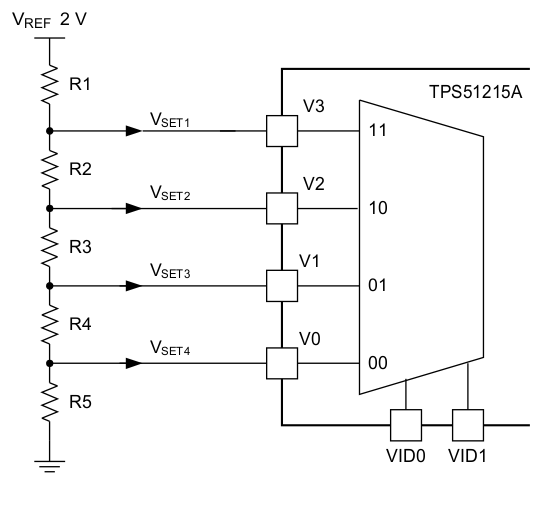
The device provides a 2.0-V, accurate voltage reference from the VREF pin. This output has a 300-µA current sourcing capability to drive V1, V2 and V3 input voltages through a voltage divider circuit as shown in Figure 7. If higher overall system accuracy is required, the sum of total resistance (R1+R2+R3+R4+R5) from VREF to GND should be designed to be more than 67 kΩ. A MLCC capacitor with a value of 0.1-µF or larger should be placed close to the VREF pin.
The device also provides 2-bit VID flexible output voltage control. Fixed 0V output voltage and up to three voltage levels can be programmed externally by a voltage divider circuit. Fixed 0V output voltage corresponds to VID 00, V1 corresponds to VID 01, V2 corresponds to VID 10 and V3 corresponds to VID 11. It is not necessary to match the voltage set point (VSET1, VSET2 or VSET3 ) to any particular V1, V2 or V3 input. Assignment of the input voltage is entirely dependent on the user requirement, which makes the device very easy and flexible to use.
The device can also be configured to provide 1-bit VID flexible output voltage operation. In the applications where fewer than four input voltage levels are needed, the remaining input voltage pins cannot be left floating.
 Figure 7. Setting the Output Voltage