SLUSCA7A
November 2015 – July 2022
TPS51216-EP
PRODUCTION DATA
1
Features
2
Applications
3
Description
4
Revision History
5
Description (continued)
6
Pin Configuration and Functions
7
Specifications
7.1
Absolute Maximum Ratings
7.2
ESD Ratings
7.3
Recommended Operating Conditions
7.4
Thermal Information
7.5
Electrical Characteristics
7.6
Typical Characteristics
8
Detailed Description
8.1
Overview
8.2
Functional Block Diagram
8.3
Feature Description
8.3.1
VDDQ Switch Mode Power Supply Control
8.3.2
VREF and REFIN, VDDQ Output Voltage
8.3.3
Soft-Start and Powergood
8.3.4
Power State Control
8.3.5
Discharge Control
8.3.6
VTT Overcurrent Protection
8.3.7
V5IN Undervoltage Lockout (UVLO) Protection
8.3.8
Thermal Shutdown
8.4
Device Functional Modes
8.4.1
MODE Pin Configuration
9
Application and Implementation
9.1
Application Information
9.1.1
D-CAP Mode
9.1.2
Light-Load Operation
9.1.3
VTT and VTTREF
9.1.4
VDDQ Overvoltage and Undervoltage Protection
9.1.5
VDDQ Overcurrent Protection
9.2
Typical Application
9.2.1
Design Requirements
9.2.2
Detailed Design Procedure
9.2.2.1
List of Materials
9.2.2.2
External Components Selection
9.2.3
Application Curve
10
Power Supply Recommendations
11
Layout
11.1
Layout Guidelines
11.2
Layout Example
12
Device and Documentation Support
12.1
Receiving Notification of Documentation Updates
12.2
Support Resources
12.3
Trademarks
12.4
Electrostatic Discharge Caution
12.5
Glossary
13
Mechanical, Packaging, and Orderable Information
Package Options
Mechanical Data (Package|Pins)
RUK|20
MPQF220D
Thermal pad, mechanical data (Package|Pins)
RUK|20
QFND191D
Orderable Information
slusca7a_oa
slusca7a_pm
9.2
Typical Application
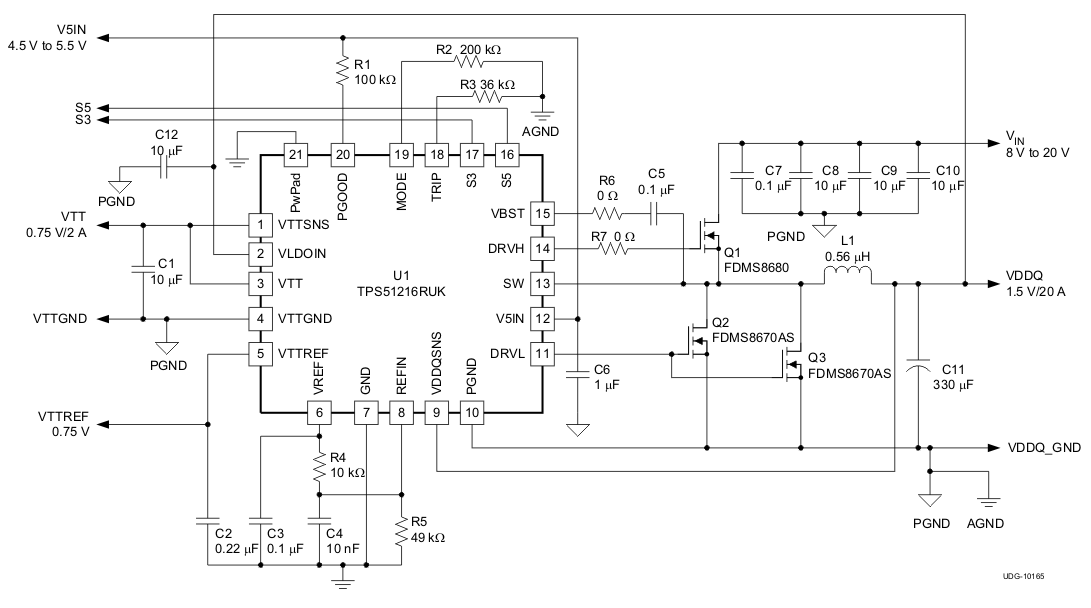
Figure 9-4
DDR3, 400-kHz Application Circuit, Tracking Discharge