SLVSCT3 March 2015 TPS51275B-1
PRODUCTION DATA.
- 1 Features
- 2 Applications
- 3 Description
- 4 Typical Application Diagram
- 5 Revision History
- 6 Pin Configuration and Functions
- 7 Specifications
-
8 Detailed Description
- 8.1 Overview
- 8.2 Functional Block Diagram
- 8.3
Feature Description
- 8.3.1 PWM Operations
- 8.3.2 Adaptive On-Time and PWM Frequency Control
- 8.3.3 Light-Load Condition in Out-of-Audio Operation
- 8.3.4 Enable and Power Good
- 8.3.5 Soft-Start and Discharge
- 8.3.6 VREG5 and VREG3 Linear Regulators
- 8.3.7 VCLK for Charge Pump
- 8.3.8 Overcurrent Protection
- 8.3.9 Output Overvoltage and Undervoltage Protection
- 8.3.10 Undervoltage Lockout Protection
- 8.3.11 Over-Temperature Protection (OTP)
- 8.4 Device Functional Modes
- 9 Application and Implementation
- 10Power Supply Recommendations
- 11Layout
- 12Device and Documentation Support
- 13Mechanical, Packaging, and Orderable Information
Package Options
Mechanical Data (Package|Pins)
- RUK|20
Thermal pad, mechanical data (Package|Pins)
- RUK|20
Orderable Information
9 Application and Implementation
NOTE
Information in the following applications sections is not part of the TI component specification, and TI does not warrant its accuracy or completeness. TI’s customers are responsible for determining suitability of components for their purposes. Customers should validate and test their design implementation to confirm system functionality.
9.1 Application Information
The TPS51275B-1 device is typically used as a dual-synchronous buck controller, which converts an input voltage ranging from 5 to 24 V, to output voltage of 5 V and 3.3 V (respectively). The device is targeted for power-supply solutions for notebook and desktop computer systems.
9.2 Typical Application
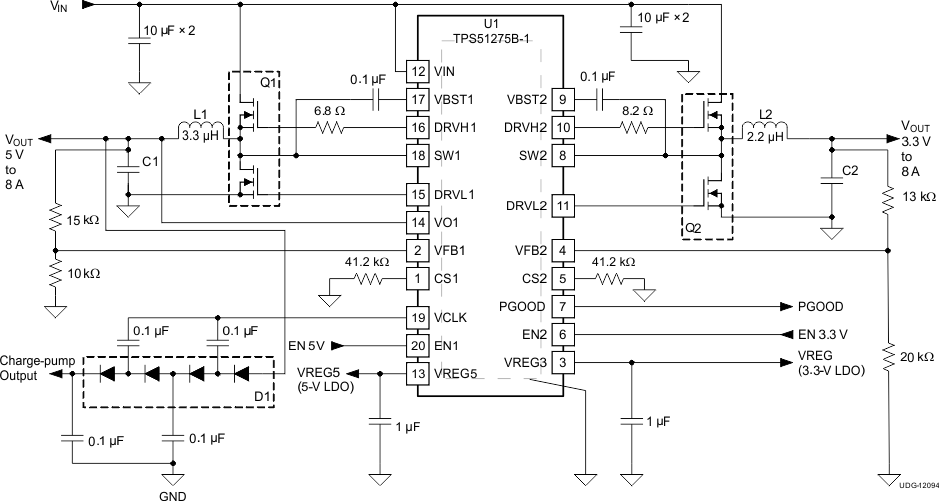 Figure 18. Detailed Application Schematic
9.2.1 Design Requirements
For this design example, use the parameters listed in Table 2.
Table 2. Design Parameters
| PARAMETER | VALUE |
|---|---|
| Input voltage range | 5.5 to 24 V |
| Channel 1 output voltage | 5 V |
| Channel 1 output voltage | 8 A |
| Channel 2 output voltage | 3.3 V |
| Channel 2 output voltage | 8 A |
9.2.2 Detailed Design Procedure
9.2.2.1 External Components Selection
The external components selection is relatively simple for a design using D-CAP mode. Table 3 lists the key external components that are recommended for this application design (see Figure 18).
Table 3. Key External Components
| REFERENCE DESIGNATOR |
FUNCTION | MANUFACTURER | PART NUMBER |
|---|---|---|---|
| L1 | Output Inductor (5 VOUT) | Alps | GLMC3R303A |
| L2 | Output Inductor (3.3 VOUT) | Alps | GLMC2R203A |
| C1 | Output Capacitor (5 VOUT) | SANYO | 6TPE220MAZB × 2 |
| C2 | Output Capacitor (3.3 VOUT) | SANYO | 6TPE220MAZB × 2 |
| Q1 | MOSFET (5 VOUT) | TI | CSD87330Q3D |
| Q2 | MOSFET (3.3 VOUT) | TI | CSD87330Q3D |
9.2.2.1.1 Step 1. Determine the Value of R1 and R2
The recommended value of R2 is between 10 kΩ and 20 kΩ. Use Equation 5 to calculate the value of R1.

9.2.2.1.2 Step 2. Select the Inductor
The inductance value should be determined to give the ripple current of approximately ½ to ¼ of maximum output current and less than half of OCL (valley) threshold. A larger ripple current increases the output ripple voltage, improves signal-to-noise ratio, and helps ensure stable operation.

The calculated inductance for channel1 and channel2 is 3.3 µH and 2 µH, respectively. For this design, select the inductance values of 3.3 µH and 2.2 µH for these two channels.
The inductor must also have low DCR to achieve good efficiency, as well as enough room above the peak inductor current before saturation. Use Equation 7 to calculate the peak inductor current.

9.2.2.1.3 Step 3. Select Output Capacitors
Organic semiconductor capacitors or specialty polymer capacitors are recommended. Determine the ESR to meet the required ripple voltage. Use Equation 8 to quickly calculate the ESR.

where
- D as the duty-cycle factor
- the required output ripple voltage slope is approximately 20 mV per tSW (switching period) in terms of the VFBx pin
The calculated minimum-required ESR for channel1 and channel2 is 9.9 mΩ and 7.8 mΩ, respectively. For this design, use two 220-µF, 35-mΩ polymer capacitors in parallel for each channel. The equivalent ESR is 17.5 mΩ which meets the minimum ESR requirement. Using a value of 440 µF for the output capacitor and 17.5 mΩ of ESR, the resulting value of the 0-dB frequency, f0 (see Equation 4), is approximately 21 kHz which is much less than fSW / 4 for both channels.
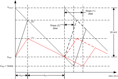 Figure 19. Ripple Voltage Slope and Jitter Performance
9.2.3 Application Curves
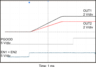
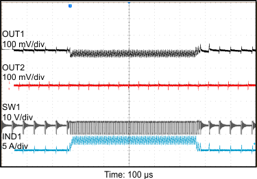
| IOUT1 = 0 to 3 A | IOUT2 = 0 A | VVIN = 7.4 V |
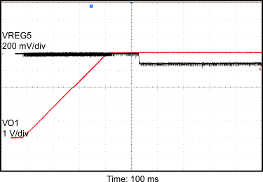
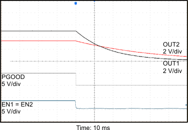
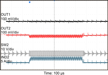
| IOUT1 = 0 A | IOUT2 = 0 to 3 A | VVIN = 7.4 V |
