SLVSCT3 March 2015 TPS51275B-1
PRODUCTION DATA.
- 1 Features
- 2 Applications
- 3 Description
- 4 Typical Application Diagram
- 5 Revision History
- 6 Pin Configuration and Functions
- 7 Specifications
-
8 Detailed Description
- 8.1 Overview
- 8.2 Functional Block Diagram
- 8.3
Feature Description
- 8.3.1 PWM Operations
- 8.3.2 Adaptive On-Time and PWM Frequency Control
- 8.3.3 Light-Load Condition in Out-of-Audio Operation
- 8.3.4 Enable and Power Good
- 8.3.5 Soft-Start and Discharge
- 8.3.6 VREG5 and VREG3 Linear Regulators
- 8.3.7 VCLK for Charge Pump
- 8.3.8 Overcurrent Protection
- 8.3.9 Output Overvoltage and Undervoltage Protection
- 8.3.10 Undervoltage Lockout Protection
- 8.3.11 Over-Temperature Protection (OTP)
- 8.4 Device Functional Modes
- 9 Application and Implementation
- 10Power Supply Recommendations
- 11Layout
- 12Device and Documentation Support
- 13Mechanical, Packaging, and Orderable Information
Package Options
Mechanical Data (Package|Pins)
- RUK|20
Thermal pad, mechanical data (Package|Pins)
- RUK|20
Orderable Information
8 Detailed Description
8.1 Overview
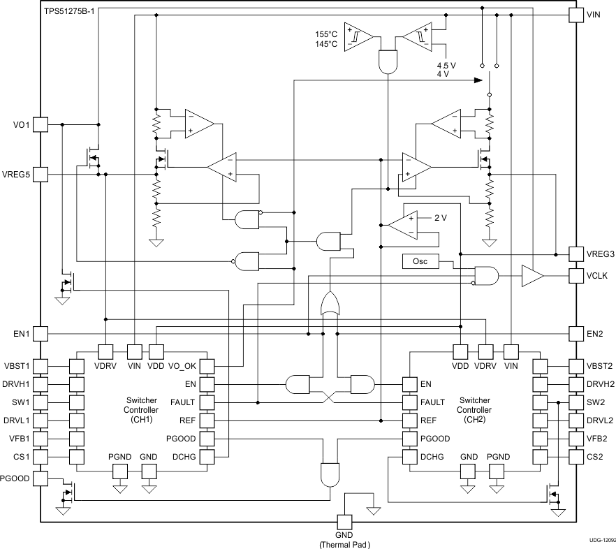
The TPS51275B-1 device is a cost-effective, dual-synchronous buck controller targeted for power-supply solutions for notebook and desktop computer systems. The device has 5-V and 3.3-V low-dropout regulators (LDOs) and requires few external components. With D-CAP control mode implemented, the compensation network can be removed. The fast transient response also reduces the output capacitance.
8.2 Functional Block Diagram

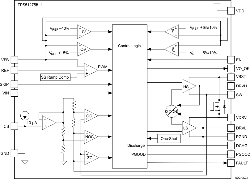
 Figure 15. Switcher Controller Block Diagram
8.3 Feature Description
8.3.1 PWM Operations
The main control loop of the switch-mode power supply (SMPS) is designed as an adaptive on-time pulse-width-modulation (PWM) controller. The control loop supports a proprietary D-CAP mode. D-CAP mode does not require an external conpensation circuit and is suitable for low external component-count configuration when used with an appropriate amount of ESR at the output capacitors.
At the beginning of each cycle, the synchronous high-side MOSFET is turned on, or enters the ON state. After the internal, one-shot timer expires, this MOSFET is turned off, or enters the OFF state. The MOSFET is turned on again when the feedback point voltage, VVFB, decreases to match the internal 2-V reference. The inductor current information is also monitored and should be below the overcurrent threshold to initiate this new cycle. By repeating the operation in this manner, the controller regulates the output voltage. The synchronous low-side (rectifying) MOSFET is turned on at the beginning of each OFF state to maintain a minimum of conduction loss. The low-side MOSFET is turned off before the high-side MOSFET turns on at next switching cycle or when inductor current information detects a zero level. When the low-side MOSFET is turned off when the inductor current detects a zero level, a seamless transition to the reduced frequency operation during light-load conditions is enabled so that high efficiency is maintained over a broad range of load current.
8.3.2 Adaptive On-Time and PWM Frequency Control
Because the TPS51275B-1 device does not have a dedicated oscillator for the on-board control loop. The switching cycle is controlled by the adaptive on-time circuit. The on-time is controlled to meet the target switching frequency by feed-forwarding the input and output voltage into the on-time one-shot timer. The target switching frequency is varied according to the input voltage to achieve higher duty operation for lower input voltage application. The switching frequency of CH1 (5-V output) is 300 kHz during continuous-conduction-mode (CCM) operation when VVIN = 20 V. The CH2 (3.3-V output) is 355 kHz during CCM when VVIN = 20 V (see Figure 13 and Figure 14).
To improve load transient performance and load regulation in lower input voltage conditions, the TPS51275B-1 device can extend the on-time. The maximum on-time extension for CH1 is 4 times and for CH2 is 3 times. To maintain a reasonable inductor ripple current during on-time extension, the inductor ripple current should be set to less than half of the OCL (valley) threshold (see the Step 2. Select the Inductor section). The on-time extension function provides high duty-cycle operation and shows better DC (static) performance. AC performance is determined mostly by the output LC filter and resistive factor in the loop.
8.3.3 Light-Load Condition in Out-of-Audio Operation
The TPS51275B-1 device automatically reduces switching frequency during light-load conditions to maintain high efficiency. This reduction of frequency is achieved smoothly and without an increase in output voltage ripple. A more detailed description of this operation follows. As the output current decreases from a heavy-load condition, the inductor current is also reduced and eventually approaches valley zero current, which is the boundary between continuous conduction mode and discontinuous conduction mode (DCM). The rectifying MOSFET is turned off when this zero inductor current is detected. As the load current further decreases, the converter runs in DCM and requires a longer and longer time to discharge the output capacitor to the level that requires the next ON cycle. The ON time is maintained the same as that in the heavy-load condition. In reverse, when the output current increases from light load to heavy load, the switching frequency increases to the preset value as the inductor current reaches to the continuous conduction. Use Equation 1 to calculate the transition load point to the light load operation IOUT(LL) (for example the threshold between continuous and discontinuous conduction mode).

where
- fSW is the PWM switching frequency
The switching frequency versus the output current during light-load conditions is a function of the inductance (L), input voltage (VVIN) and output voltage (VOUT), but it decreases almost proportional to the output current from the IOUT(LL). As the load current continues to decrease, the switching frequency can decrease into the acoustic audible frequency range. To prevent this from happening, Out-of-Audio (OOA) light-load mode is implemented.
During Out-of-Audio operation, the OOA control circuit monitors the states of both the high-side and low-side MOSFETs and forces them switching if both MOSFETs are off for more than 40 µs. When both high-side and low-side MOSFETs are off for 40 µs during a light-load condition, the operation mode is changed to forced CCM (FCCM). This mode change initiates one cycle of turning on both the low-side MOSFET and the high-side MOSFET. Then, both MOSFETs remain turned off waiting for another 40 µs.
8.3.4 Enable and Power Good
The VREG3 and VREG5 pins are always-on regulators, when the input voltage is beyond the UVLO threshold it turns ON. The VCLK signal initiates when the EN1 pin enters the ON state. Table 1 lists the enable states.
Table 1. Enabling and PGOOD State
| EN1 | EN2 | VREG5 | VREG3 | CH1 (5 VOUT) | CH2 (3.3 VOUT) | VCLK | PGOOD |
|---|---|---|---|---|---|---|---|
| OFF | OFF | ON | ON | OFF | OFF | OFF | Low |
| ON | OFF | ON | ON | ON | OFF | ON | Low |
| OFF | ON | ON | ON | OFF | ON | OFF | Low |
| ON | ON | ON | ON | ON | ON | ON | High |
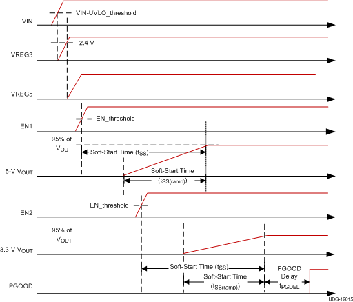
 Figure 16. Timing Diagram
8.3.5 Soft-Start and Discharge
The TPS51275B-1 device operates an internal, 3.2-ms, voltage servo soft-start for each channel. When the ENx pin becomes higher than the enable threshold voltage, an internal DAC begins ramping up the reference voltage to the PWM comparator. Smooth control of the output voltage is maintained during startup. When the ENx pin becomes lower than the lower level of threshold voltage, the TPS51275B-1 device discharges the outputs using internal MOSFETs through VO1 (CH1) and SW2 (CH2).
8.3.6 VREG5 and VREG3 Linear Regulators
The two sets of 100-mA standby linear regulators output 5 V and 3.3 V, respectively. The VREG5 pin provides the current for the gate drivers. The VREG3 pin functions as the main power supply for the analog circuitry of the device. Both the VREG5 and VREG3 regulators are always-ON LDOs (see Table 1).
To stabilize regulators, add ceramic capacitors with a value of 1 µF or larger (X5R grade or better) placed close to the VREG5 and VREG3 pins.
The VREG5 pin switchover function is asserted when the following three conditions are present:
- CH1 internal PGOOD is high
- CH1 is not in overcurrent-limit (OCL) condition
- VO1 voltage is higher than VREG5-1V
In this switchover condition the following three things occur:
- The internal 5-V LDO regulator is shut off
- The VREG5 output is connected to VO1 by internal switchover MOSFET
- VREG3 input pass is changed from VIN to VO1
8.3.7 VCLK for Charge Pump
The 260-kHz VCLK signal can be used in the charge pump circuit. The VCLK signal becomes available when the EN1 pin is in the ON state. The VCLK driver is driven by the VO1 voltage. In a design that does not require VCLK output, leave the VCLK pin open.
8.3.8 Overcurrent Protection
The TPS51275B-1 device has cycle-by-cycle overcurrent limiting control. The inductor current is monitored during the OFF state and the controller maintains the OFF state during the inductor current is larger than the overcurrent trip level. To provide both good accuracy and a cost effective solution, the TPS51275B-1 device supports temperature-compensated MOSFET RDS(on) sensing. Connect the CSx pin to ground (GND) through the CS voltage setting resistor, RCS. The CSx pin sources CS current (ICS) which is 10 µA typically at room temperature, and the CSx terminal voltage (VCS= RCS × ICS) should be in the range of 0.2 to 2 V over all operation temperatures. The trip level is set to the OCL trip voltage (VTRIP) as shown in Equation 2.

The inductor current is monitored by the voltage between the GND and the SWx pin so that SWx pin is connected to the drain terminal of the low-side MOSFET properly. The CS pin current has a 4500 ppm/°C temperature slope to compensate the temperature dependency of the RDS(on). GND is used as the positive current sensing node so that GND should be connected to the source terminal of the low-side MOSFET.
As the comparison is done during the OFF state, VTRIP sets the valley level of the inductor current. Thus, the load current at the overcurrent threshold, IOCP, can be calculated as shown in Equation 3.

In an overcurrent condition, the current to the load exceeds the current to the output capacitor and therefore the output voltage tends to fall down. Eventually, the output voltage ends up crossing the undervoltage protection threshold and both channels shut down.
8.3.9 Output Overvoltage and Undervoltage Protection
The TPS51275B-1 device asserts the overvoltage protection (OVP) when the VFBx voltage reaches the OVP-trip threshold level. When an OVP event is detected, the controller changes the output target voltage to 0 V which usually turns off the DRVHx pin and forces the DRVLx pin to turn on. When the inductor current begins to flow through the low-side MOSFET and reaches the negative OCL, the DRVLx pin is turned off and the DRVHx pin is turned on. After the on-time expires, the DRVHx pin is turned off and the DRVLx pin is turned on again. This action minimizes the output node undershoot because of LC resonance. When the VFBx pin reaches 0 V, the driver output is latched as the DRVHx pin turns off, the DRVLx pin turns on. The undervoltage protection (UVP) latch is set when the VFBx voltage remains lower than UVP trip threshold voltage for 250 µs or longer. In this fault condition, the controller latches the DRVHx and DRVLx pins low and discharges the outputs. The UVP detection function is enabled after 4.3 ms of SMPS operation to ensure startup.
8.3.10 Undervoltage Lockout Protection
The TPS51275B-1 device has undervoltage lockout (UVLO) protection at the VIN, VREG5, and VREG3 pins. When each voltage is lower than the respective UVLO threshold voltage, both SMPSs are shut-off. The UNVLO is a non-latch protection.
8.3.11 Over-Temperature Protection (OTP)
The TPS51275B-1 device features an internal temperature monitor. If the temperature exceeds the threshold value (typically 155°C), the TPS51275B-1 device, including the regulators, shuts off. The OTP is anon-latch protection.
8.4 Device Functional Modes
8.4.1 D-CAP Mode
From small-signal loop analysis, a buck converter using D-CAP mode can be simplified as shown in Figure 17.
 Figure 17. Simplifying the Modulator
The output voltage is compared with the internal reference voltage after the divider resistors, R1 and R2. The PWM comparator determines the timing to turn on the high-side MOSFET. The gain and speed of the comparator is high enough to keep the voltage at the beginning of each ON cycle substantially constant. For the loop stability, the 0-dB frequency, ƒ0, defined in Equation 4 must be lower than 1/4 of the switching frequency.

As ƒ0 is determined solely by the output capacitor characteristics, the loop stability during D-CAP mode is determined by the capacitor chemistry. For example, specialty polymer capacitors have output capacitance in the order of several hundred micro-Farads and ESR in range of 10 mΩ. These capacitors yield an f0 value on the order of 100 kHz or less and the loop is stable. However, ceramic capacitors have ƒ0 at more than 700 kHz, which is not suitable for this operational mode.