SLUSAE1F December 2010 – December 2018 TPS51916
PRODUCTION DATA.
- 1 Features
- 2 Applications
- 3 Description
- 4 Revision History
- 5 Pin Configuration and Functions
- 6 Specifications
-
7 Detailed Description
- 7.1 Overview
- 7.2 Functional Block Diagram
- 7.3
Feature Description
- 7.3.1 VDDQ Switch Mode Power Supply Control
- 7.3.2 VREF and REFIN, VDDQ Output Voltage
- 7.3.3 Soft-Start and Powergood
- 7.3.4 Power State Control
- 7.3.5 Discharge Control
- 7.3.6 VTT and VTTREF
- 7.3.7 VDDQ Overvoltage and Undervoltage Protection
- 7.3.8 VDDQ Out-of-Bound Operation
- 7.3.9 VDDQ Overcurrent Protection
- 7.3.10 VTT Overcurrent Protection
- 7.3.11 V5IN Undervoltage Lockout Protection
- 7.3.12 Thermal Shutdown
- 7.4 Device Functional Modes
- 7.5 D-CAP2™ Mode Operation
- 8 Application and Implementation
- 9 Power Supply Recommendations
- 10Layout
- 11Device and Documentation Support
- 12Mechanical, Packaging, and Orderable Information
Package Options
Mechanical Data (Package|Pins)
- RUK|20
Thermal pad, mechanical data (Package|Pins)
- RUK|20
Orderable Information
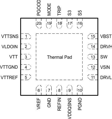
5 Pin Configuration and Functions
RUK Package
20-Pin QFN
Top View

Pin Functions
| PIN | I/O | DESCRIPTION | |
|---|---|---|---|
| NAME | NO. | ||
| DRVH | 14 | O | High-side MOSFET gate driver output. |
| DRVL | 11 | O | Low-side MOSFET gate driver output. |
| GND | 7 | – | Signal ground. |
| MODE | 19 | I | Connect resistor to GND to configure switching frequency, control mode and discharge mode. (See Table 2) |
| PGND | 10 | – | Gate driver power ground. RDS(on) current sensing input(+). |
| PGOOD | 20 | O | Powergood signal open drain output. PGOOD goes high when VDDQ output voltage is within the target range. |
| REFIN | 8 | I | Reference input for VDDQ. Connect to the midpoint of a resistor divider from VREF to GND. Add a capacitor for stable operation. |
| SW | 13 | I/O | High-side MOSFET gate driver return. RDS(on) current sensing input(–). |
| S3 | 17 | I | S3 signal input. (See Table 1) |
| S5 | 16 | I | S5 signal input. (See Table 1) |
| TRIP | 18 | I | Connect resistor to GND to set OCL at VTRIP/8. Output 10-μA current at room temperature, TC = 4700 ppm/°C. |
| VBST | 15 | I | High-side MOSFET gate driver bootstrap voltage input. Connect a capacitor from the VBST pin to the SW pin. |
| VDDQSNS | 9 | I | VDDQ output voltage feedback. Reference input for VTTREF. Also serves as power supply for VTTREF. |
| VLDOIN | 2 | I | Power supply input for VTT LDO. Connect VDDQ in typical application. |
| VREF | 6 | O | 1.8-V reference output. |
| VTT | 3 | O | VTT 2-A LDO output. Need to connect at least 10 μF of capacitance for stability. |
| VTTGND | 4 | – | Power ground for VTT LDO. |
| VTTREF | 5 | O | Buffered VTT reference output. Need to connect 0.22 μF or larger capacitance for stability. |
| VTTSNS | 1 | I | VTT output voltage feedback. |
| V5IN | 12 | I | 5-V power supply input for internal circuits and MOSFET gate drivers. |
| Thermal pad | – | Thermal pad. Connect directly to system GND plane with multiple vias. | |