SLUSD61A December 2017 – March 2019 TPS53119
PRODUCTION DATA.
- 1 Features
- 2 Applications
- 3 Description
- 4 Revision History
- 5 Pin Configuration and Functions
- 6 Specifications
-
7 Detailed Description
- 7.1 Overview
- 7.2 Functional Block Diagram
- 7.3
Feature Description
- 7.3.1 Enable and Soft-Start
- 7.3.2 Adaptive ON-Time D-CAP Control and Frequency Selection
- 7.3.3 Small Signal Model
- 7.3.4 Ramp Signal
- 7.3.5 Adaptive Zero Crossing
- 7.3.6 Output Discharge Control
- 7.3.7 Low-Side Driver
- 7.3.8 High-Side Driver
- 7.3.9 Power Good
- 7.3.10 Current Sense and Overcurrent Protection
- 7.3.11 Overvoltage and Undervoltage Protection
- 7.3.12 UVLO Protection
- 7.3.13 Thermal Shutdown
- 7.4 Device Functional Modes
- 8 Application and Implementation
- 9 Power Supply Recommendations
- 10Layout
- 11Device and Documentation Support
- 12Mechanical, Packaging, and Orderable Information
Package Options
Mechanical Data (Package|Pins)
- RGT|16
Thermal pad, mechanical data (Package|Pins)
- RGT|16
Orderable Information
10.2 Layout Example
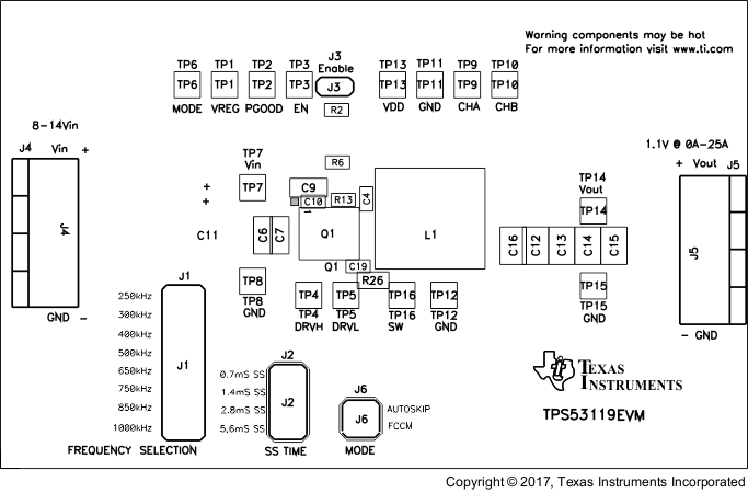 Figure 26. TPS53119EVM-690 Top Layer Assembly Drawing, Top View
 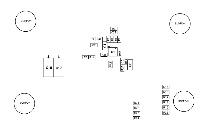 Figure 27. TPS53119EVM-690 Bottom Assembly Drawing, Bottom View
 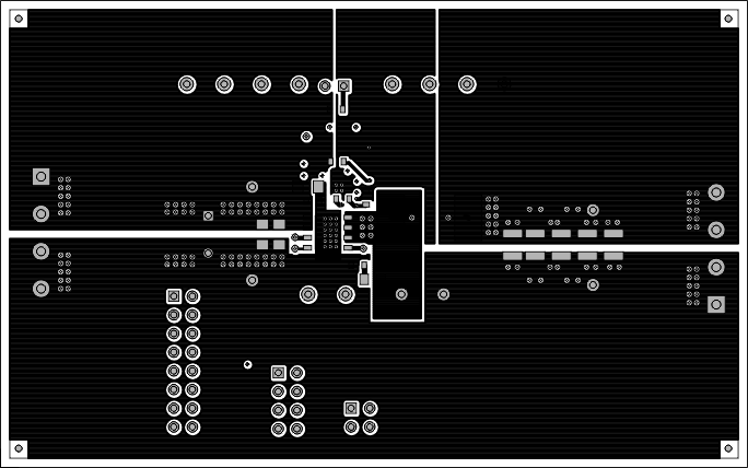 Figure 28. TPS53119EVM-690 Top Copper, Top View
 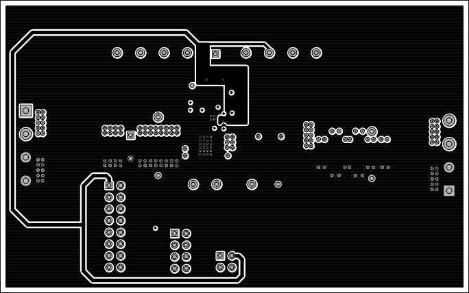 Figure 29. TPS53119EVM-690 Layer-2 Copper, Top View
 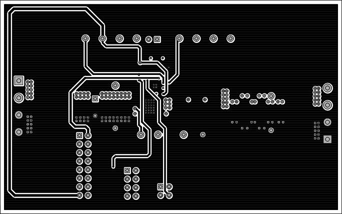 Figure 30. TPS53119EVM-690 Layer-3 Copper, Top View
 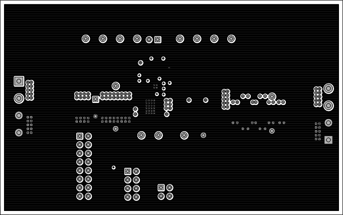 Figure 31. TPS53119EVM-690 Layer-4 Copper, Top View
  Figure 32. TPS53119EVM-690 Layer-5 Copper, Top View
 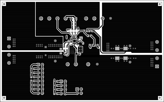 Figure 33. TPS53119EVM-690 Bottom Layer Copper, Top View