SLUSD61A December 2017 – March 2019 TPS53119
PRODUCTION DATA.
- 1 Features
- 2 Applications
- 3 Description
- 4 Revision History
- 5 Pin Configuration and Functions
- 6 Specifications
-
7 Detailed Description
- 7.1 Overview
- 7.2 Functional Block Diagram
- 7.3
Feature Description
- 7.3.1 Enable and Soft-Start
- 7.3.2 Adaptive ON-Time D-CAP Control and Frequency Selection
- 7.3.3 Small Signal Model
- 7.3.4 Ramp Signal
- 7.3.5 Adaptive Zero Crossing
- 7.3.6 Output Discharge Control
- 7.3.7 Low-Side Driver
- 7.3.8 High-Side Driver
- 7.3.9 Power Good
- 7.3.10 Current Sense and Overcurrent Protection
- 7.3.11 Overvoltage and Undervoltage Protection
- 7.3.12 UVLO Protection
- 7.3.13 Thermal Shutdown
- 7.4 Device Functional Modes
- 8 Application and Implementation
- 9 Power Supply Recommendations
- 10Layout
- 11Device and Documentation Support
- 12Mechanical, Packaging, and Orderable Information
Package Options
Mechanical Data (Package|Pins)
- RGT|16
Thermal pad, mechanical data (Package|Pins)
- RGT|16
Orderable Information
6.6 Typical Characteristics
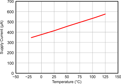 Figure 1. VDD Supply Current vs Temperature
 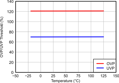 Figure 3. OVP/UVP Threshold vs Temperature
 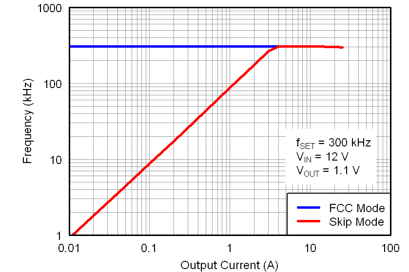 Figure 5. Switching Frequency vs Output Current
 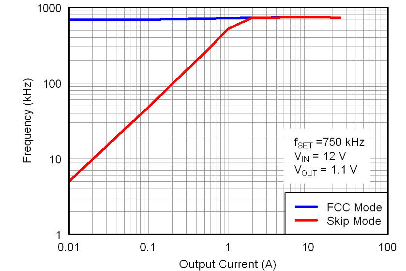 Figure 7. Switching Frequency vs Output Current
 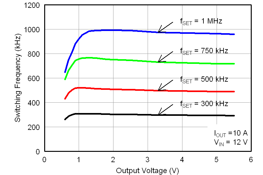 Figure 9. Switching Frequency vs Output Voltage
 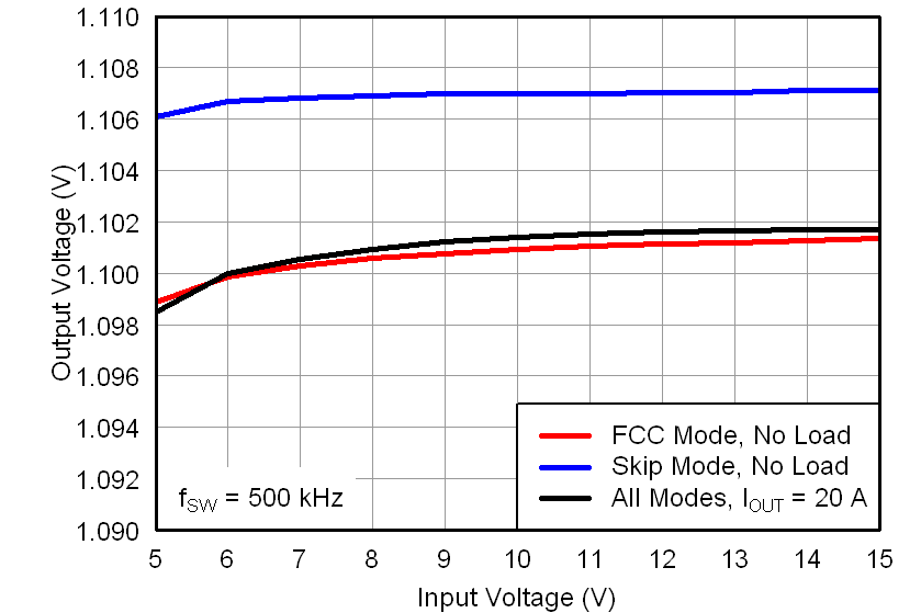 Figure 11. Output Voltage vs Input Voltage
 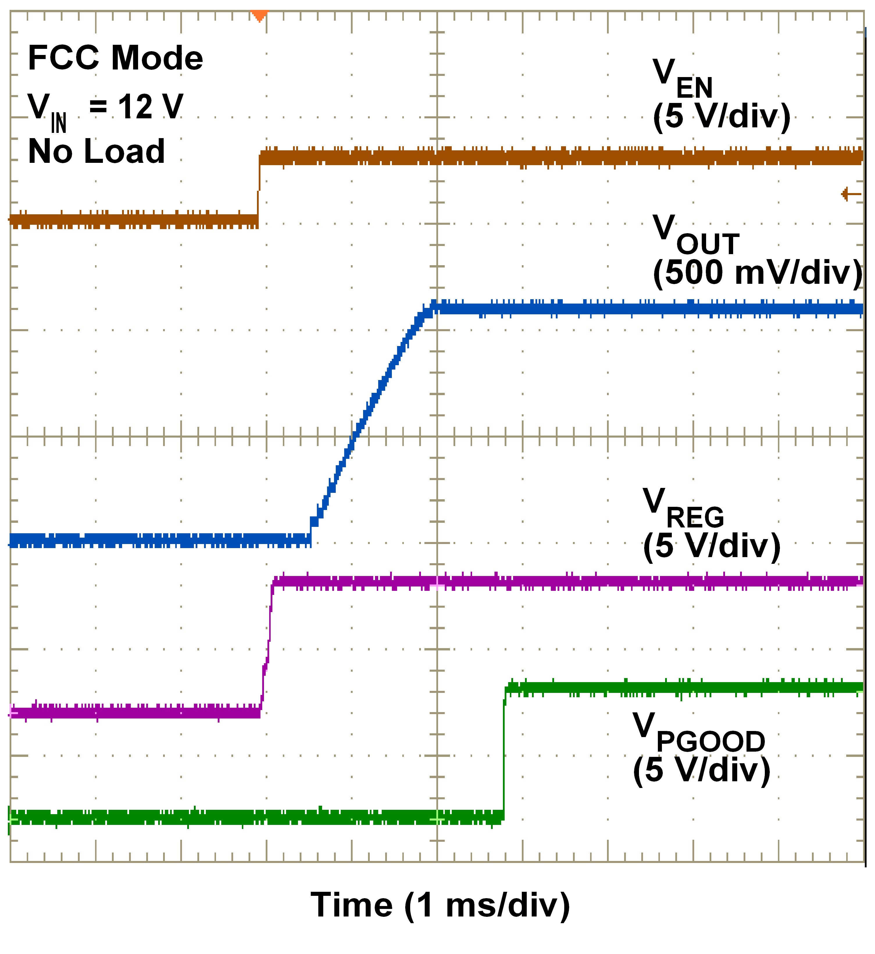 Figure 13. Start-Up Waveform
 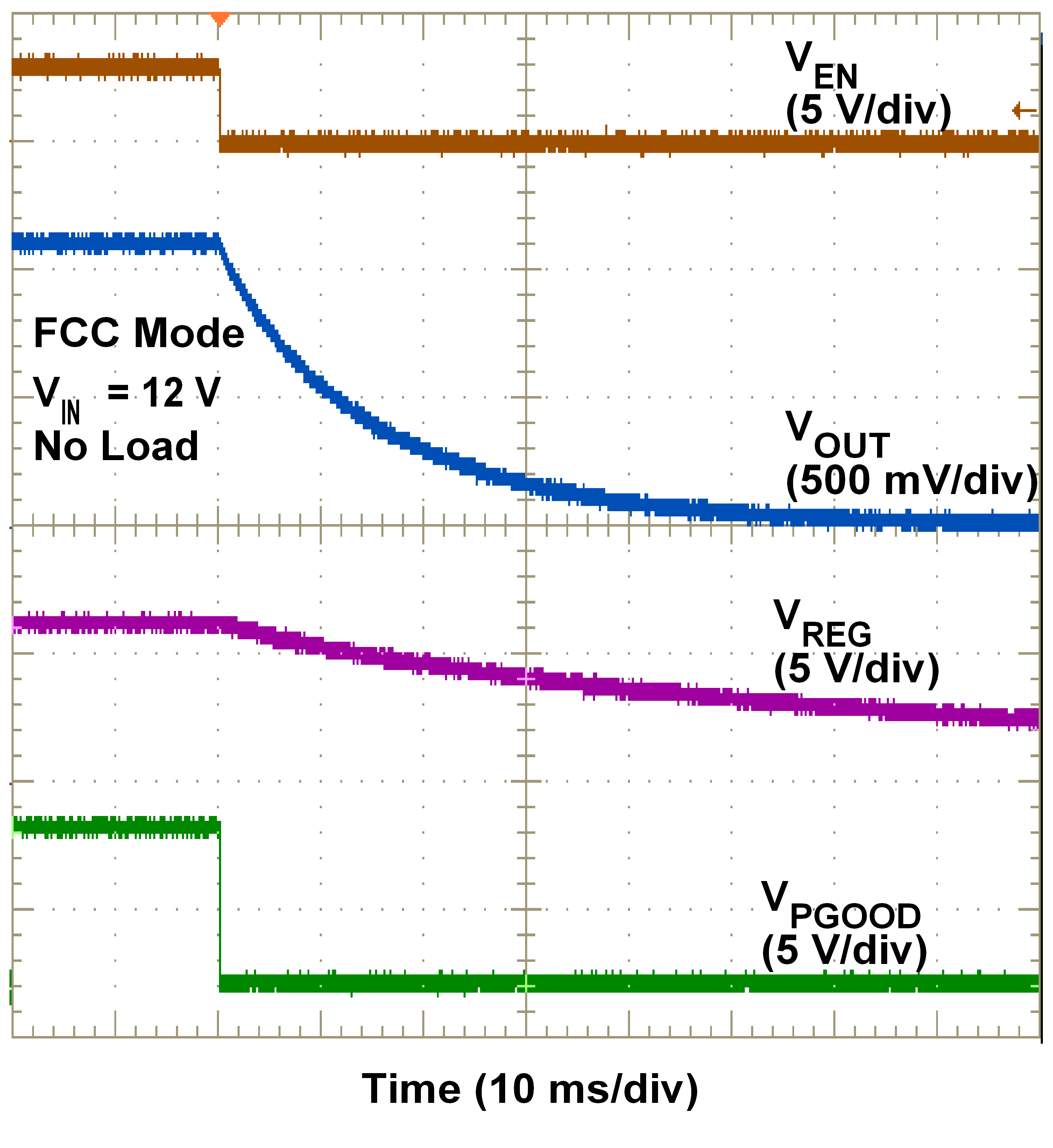 Figure 15. Turnoff Waveform
 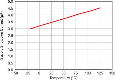 Figure 2. VDD Shutdown Current vs Temperature
  Figure 4. TRIP Pin Current vs Temperature
 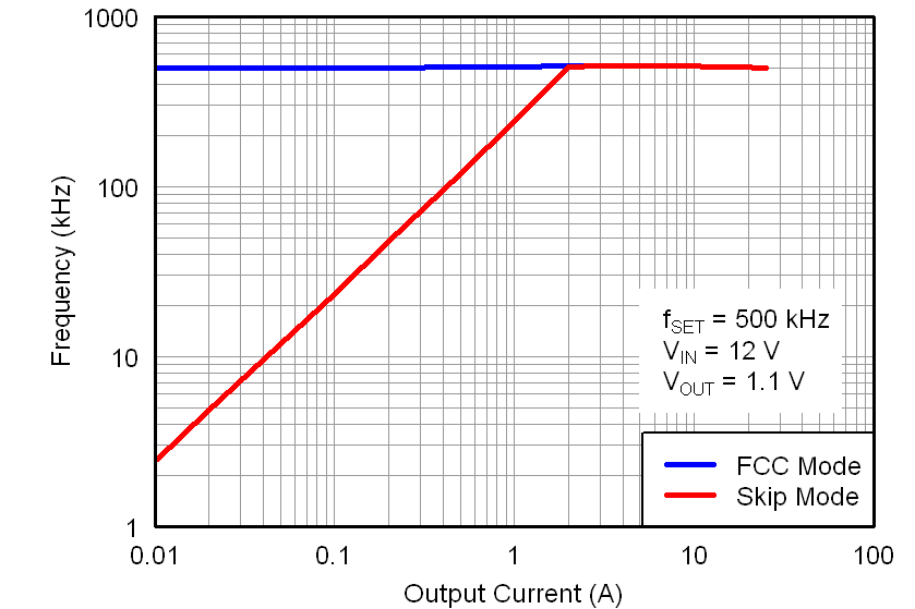 Figure 6. Switching Frequency vs Output Current
 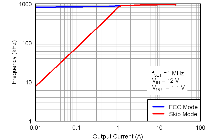 Figure 8. Switching Frequency vs Output Current
 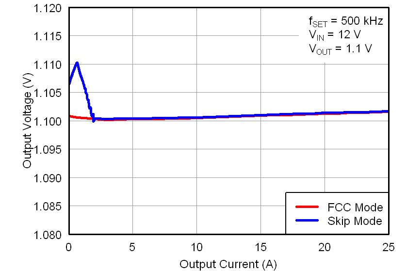 Figure 10. Output Voltage vs Output Current
 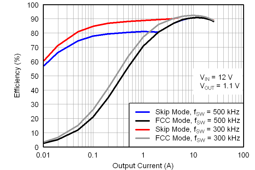 Figure 12. Efficiency vs Output Current
 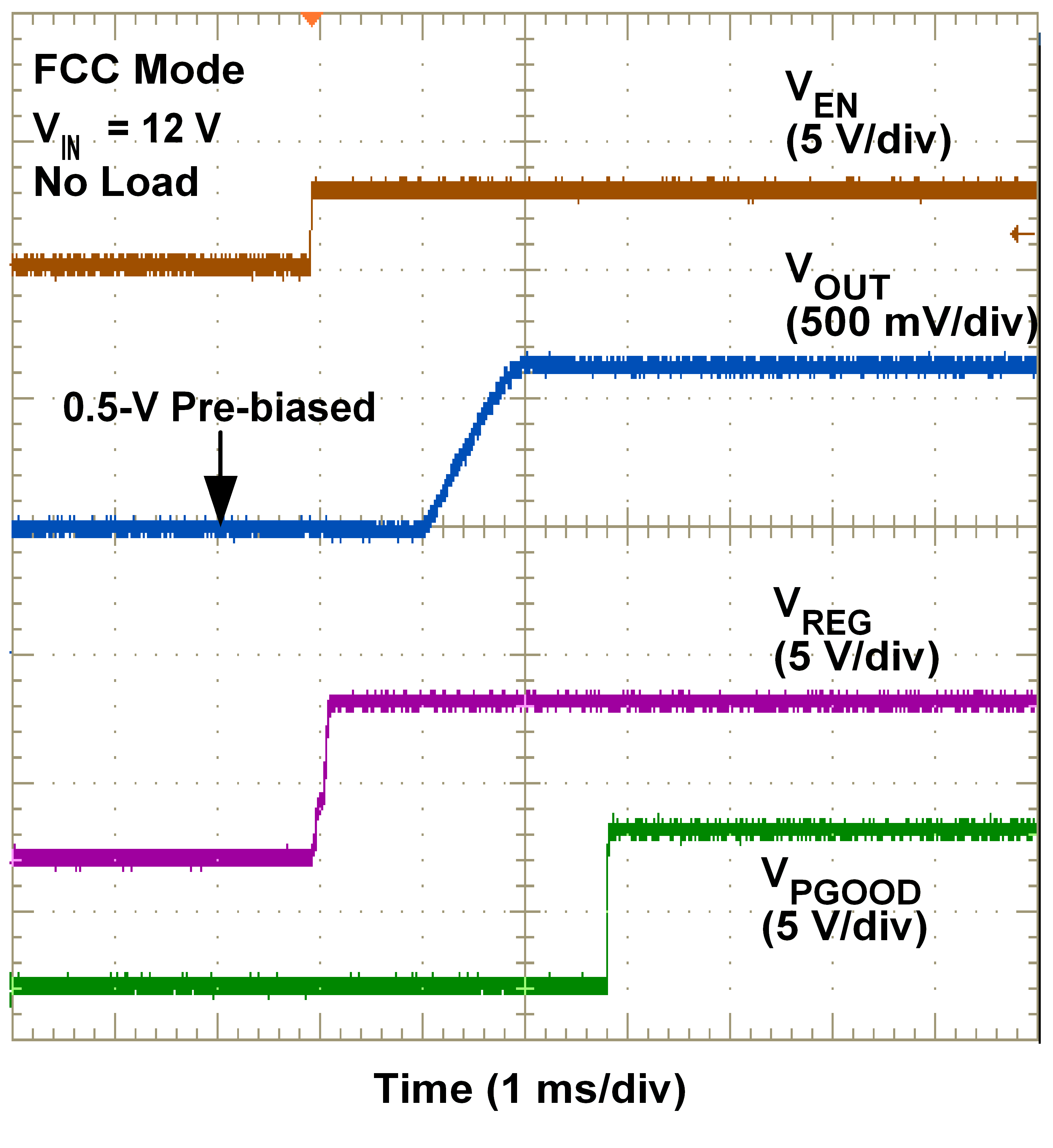 Figure 14. Prebias Start-Up Waveform
 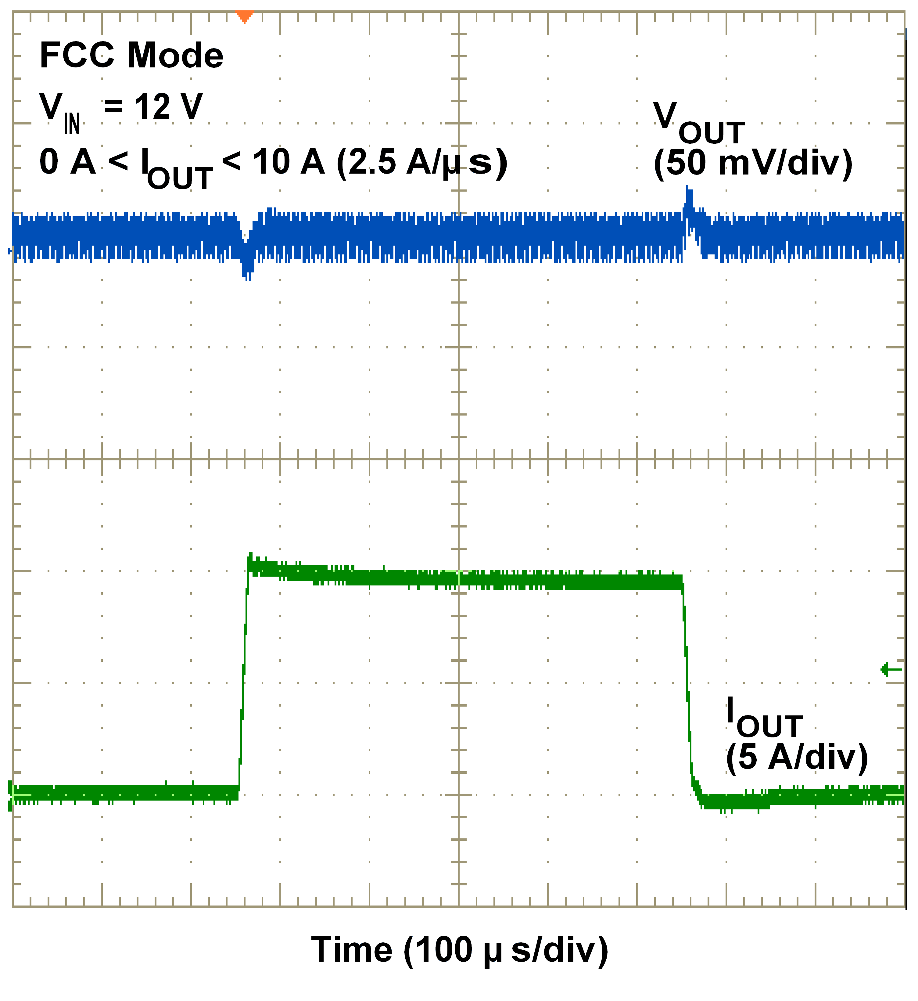 Figure 16. Load Transient Response