SLUSAS8A December 2011 – October 2016 TPS53313
PRODUCTION DATA.
- 1 Features
- 2 Applications
- 3 Description
- 4 Revision History
- 5 Pin Configuration and Functions
- 6 Specifications
- 7 Detailed Description
- 8 Application and Implementation
- 9 Power Supply Recommendations
- 10Layout
- 11Device and Documentation Support
- 12Mechanical, Packaging, and Orderable Information
Package Options
Mechanical Data (Package|Pins)
- RGE|24
Thermal pad, mechanical data (Package|Pins)
- RGE|24
Orderable Information
8 Application and Implementation
NOTE
Information in the following applications sections is not part of the TI component specification, and TI does not warrant its accuracy or completeness. TI’s customers are responsible for determining suitability of components for their purposes. Customers should validate and test their design implementation to confirm system functionality.
8.1 Application Information
The TPS53313 device is a high-efficiency synchronous-buck converter. The device suits low output voltage point-of-load applications with 6-A or lower output current in computing and similar digital consumer applications.
8.2 Typical Application
This design example describes a voltage-mode, 6-A synchronous buck converter with integrated MOSFETs. The device provides a fixed 1.2-V output at up to 6-A from a 12-V input bus.
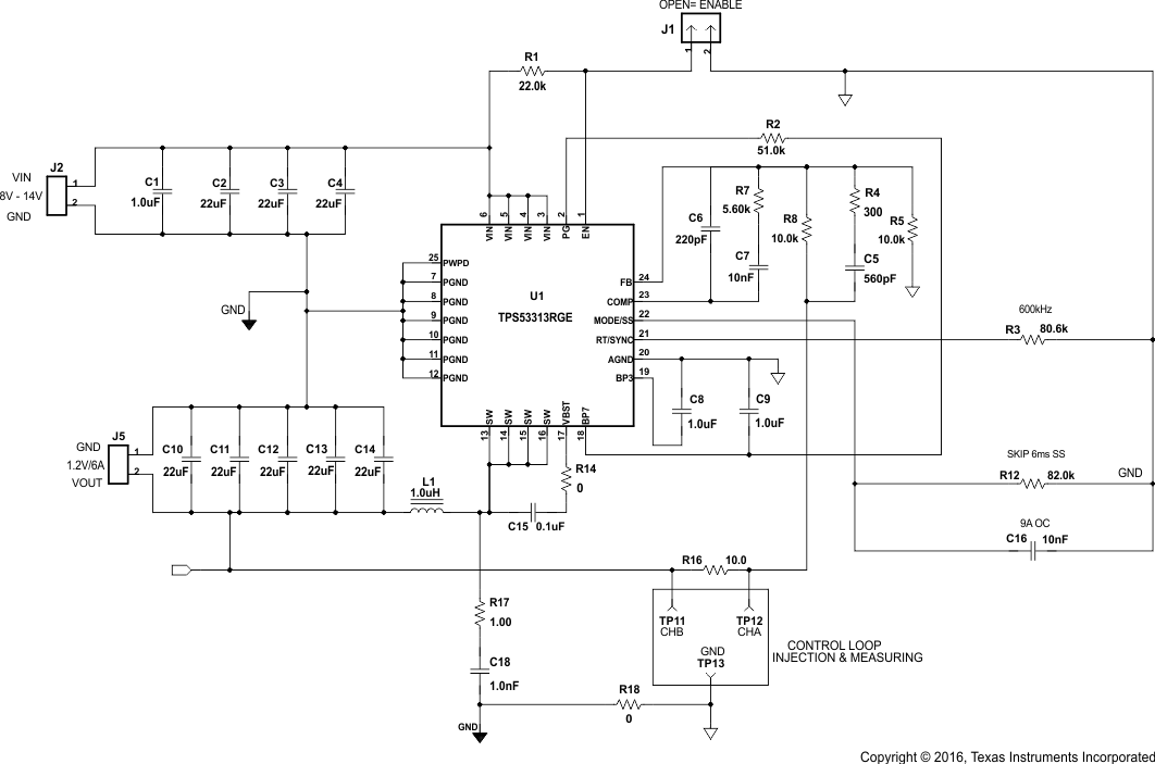 Figure 13. Typical Application Schematic
8.2.1 Design Requirements
This design example illustrates the design process and component selection for a single-output synchronous buck converter using the TPS53313. The design example schematic of a is shown in Figure 13. The specification of the converter is listed in Table 3.
Table 3. Design Example Converter Specifications
| PARAMETER | TEST CONDITION | MIN | TYP | MAX | UNIT | |
|---|---|---|---|---|---|---|
| VIN | Input voltage | 10.8 | 12 | 13.2 | V | |
| VOUT | Output voltage | 1.2 | V | |||
| VRIPPLE | Output ripple | IOUT = 6 A | 1% of VOUT | V | ||
| IOUT | Output current | 6 | A | |||
| fSW | Switching frequency | 600 | kHz | |||
8.2.2 Detailed Design Procedure
8.2.2.1 Output Inductor Selection
The inductance value should be determined to give the ripple current of approximately 20% to 40% of maximum output current. The inductor ripple current is determined by Equation 1.

The inductor also requires a low DCR to achieve good efficiency, as well as enough room above peak inductor current before saturation.
8.2.2.2 Output Capacitor Selection
The output capacitor selection is determined by output ripple and transient requirement. When operating in CCM, the output ripple has three components:


When ceramic output capacitor is chosen, the ESL component is usually negligible. In the case when multiple output capacitors are used, the total ESR and ESL should be the equivalent of the all output capacitors in parallel.
When operating in DCM, the output ripple is dominated by the component determined by capacitance. It also varies with load current and can be expressed as shown in Equation 6.

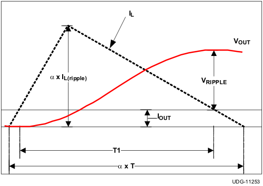 Figure 14. DCM Output Voltage Ripple
8.2.2.3 Input Capacitor Selection
The selection of input capacitor should be determined by the ripple current requirement. The ripple current generated by the converter needs to be absorbed by the input capacitors as well as the input source. The RMS ripple current from the converter can be expressed as shown in Equation 8.

To minimize the ripple current drawn from the input source, sufficient input decoupling capacitors should be placed close to the device. The ceramic capacitor is recommended due to its low ESR and low ESL. The input voltage ripple can be calculated as below when the total input capacitance is determined by Equation 10.

8.2.2.4 Output Voltage Setting Resistors Selection
The output voltage is programmed by the voltage-divider resistor, R1 and R2 shown in Equation 11. R1 is connected between VFB pin and the output, and R2 is connected between the VFB pin and GND. Recommended value for R1 is from 1k to 5k. Determine R2 using Equation 11.

8.2.2.5 Compensation Design
The TPS53313 employs voltage mode control. To effectively compensate the power stage and ensure fast transient response, Type III compensation is typically used.

The output LC filter introduces a double pole which can be calculated as shown in Equation 13.

The ESR zero of can be calculated as shown in Equation 14.

Figure 15 and Figure 16 shows the configuration of Type III compensation and typical pole and zero locations. Equation 15 through Equation 17 describe the compensator transfer function and poles and zeros of the Type III network.


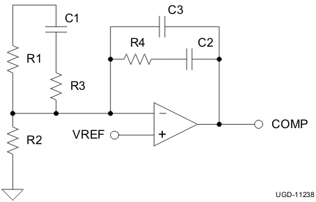 Figure 15. Type III Compensation
Network Schematic
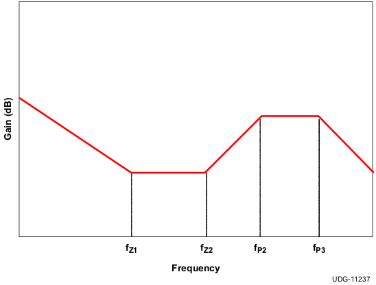 Figure 16. Type III Compensation
Network Waveform


The two zeros can be placed near the double pole frequency to cancel the response from the double pole. One pole can be used to cancel ESR zero, and the other non-zero pole can be placed at half switching frequency to attenuate the high frequency noise and switching ripple. Suitable values can be selected to achieve a compromise between high phase margin and fast response. A phase margin higher than 45° is required for stable operation.
For DCM operation, a capacitor with a value between 100 pF and 220 pF is recommended for C3 when the output capacitance is between 22 µF and 220 µF.
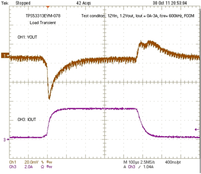
8.2.3 Application Curves
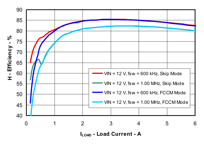 Figure 17. Efficiency
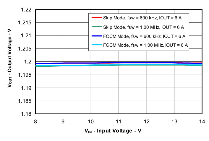
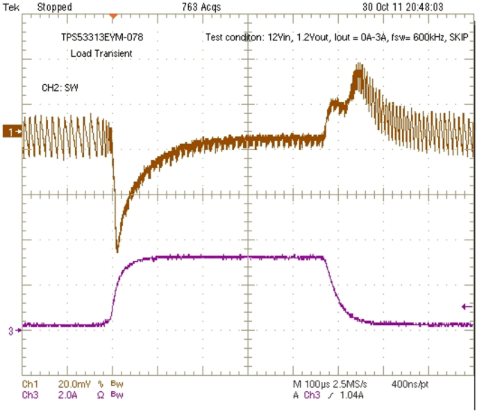
Under Skip Mode
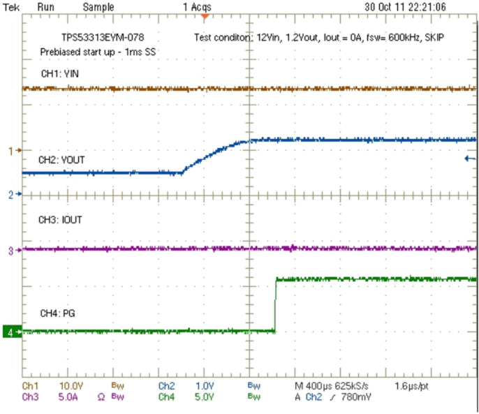
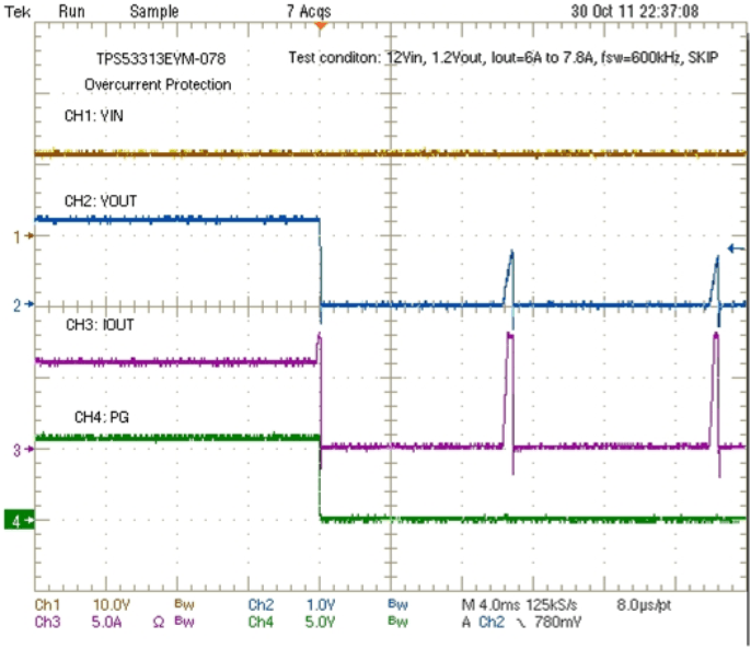
| 12-V VIN, 1.2-V VOUT, IOUT increases from 6 A to 7.8 A | ||||
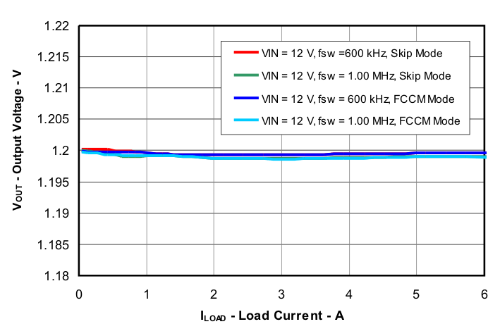 Figure 18. Load Regulation
Under FCCM Mode
