SLUSAS8A December   2011  – October 2016 TPS53313

PRODUCTION DATA.  

  1. Features
  2. Applications
  3. Description
  4. Revision History
  5. Pin Configuration and Functions
  6. Specifications
    1. 6.1 Absolute Maximum Ratings
    2. 6.2 ESD Ratings
    3. 6.3 Recommended Operating Conditions
    4. 6.4 Thermal Information
    5. 6.5 Electrical Characteristics
    6. 6.6 Typical Characteristics
  7. Detailed Description
    1. 7.1 Overview
    2. 7.2 Functional Block Diagram
    3. 7.3 Feature Description
      1. 7.3.1 Soft-Start Operation
      2. 7.3.2 Power Good
      3. 7.3.3 UVLO Function
      4. 7.3.4 Overcurrent (OC) Protection
      5. 7.3.5 Overvoltage and Undervoltage Protection
      6. 7.3.6 Overtemperature Protection
      7. 7.3.7 Output Discharge
      8. 7.3.8 Switching Frequency Setting and Synchronization
    4. 7.4 Device Functional Modes
      1. 7.4.1 Operation Mode
      2. 7.4.2 Light Load Operation
      3. 7.4.3 Forced Continuous Conduction Mode
  8. Application and Implementation
    1. 8.1 Application Information
    2. 8.2 Typical Application
      1. 8.2.1 Design Requirements
      2. 8.2.2 Detailed Design Procedure
        1. 8.2.2.1 Output Inductor Selection
        2. 8.2.2.2 Output Capacitor Selection
        3. 8.2.2.3 Input Capacitor Selection
        4. 8.2.2.4 Output Voltage Setting Resistors Selection
        5. 8.2.2.5 Compensation Design
      3. 8.2.3 Application Curves
  9. Power Supply Recommendations
  10. 10Layout
    1. 10.1 Layout Guidelines
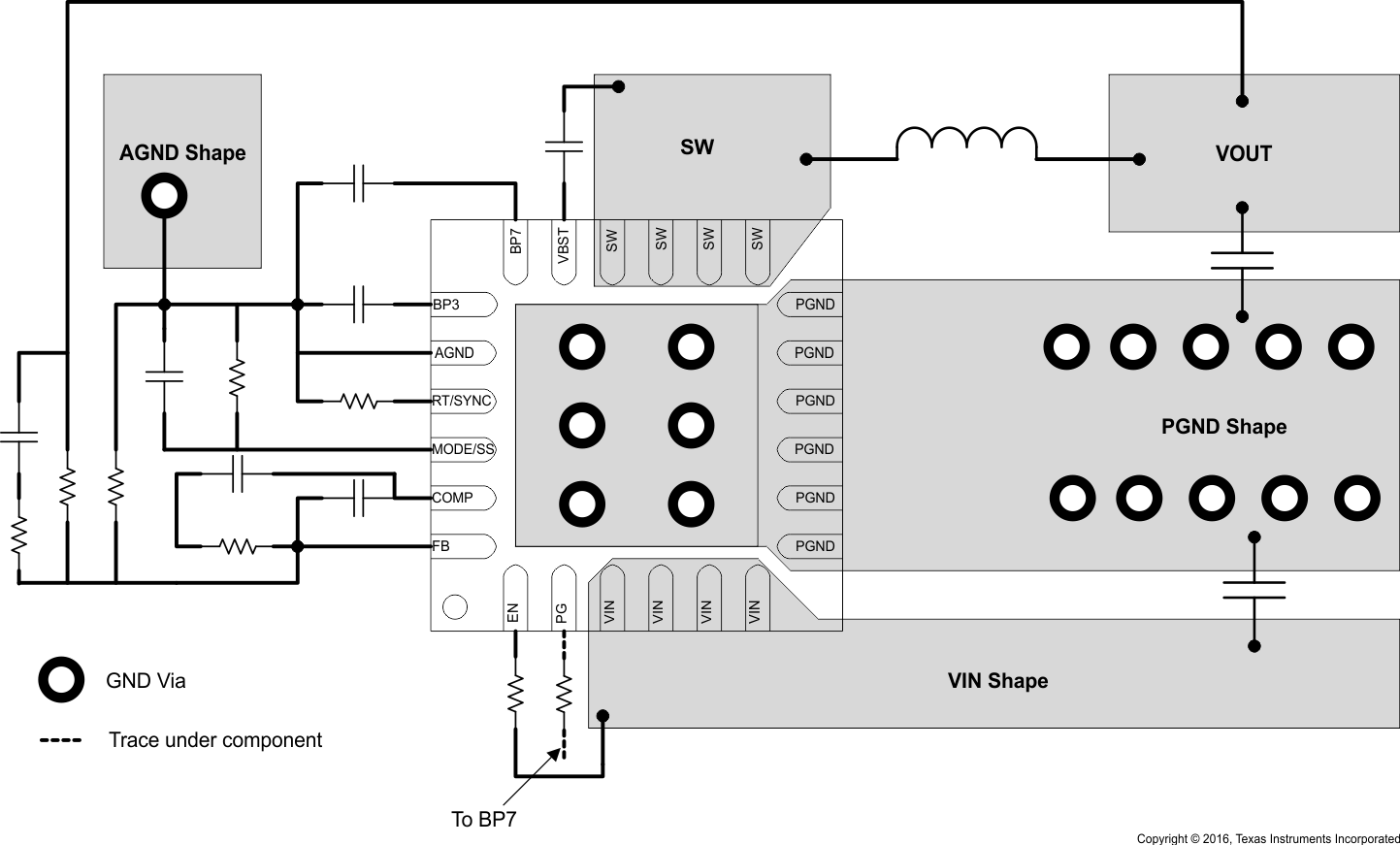
    2. 10.2 Layout Example
  11. 11Device and Documentation Support
    1. 11.1 Receiving Notification of Documentation Updates
    2. 11.2 Community Resources
    3. 11.3 Trademarks
    4. 11.4 Electrostatic Discharge Caution
    5. 11.5 Glossary
  12. 12Mechanical, Packaging, and Orderable Information

Package Options

Mechanical Data (Package|Pins)
Thermal pad, mechanical data (Package|Pins)
Orderable Information

Layout

Layout Guidelines

Good layout is essential for stable power supply operation. Follow these guidelines for an efficient PCB layout:

  • Separate the power ground and analog ground planes. Connect them together at one location.
  • Use 6 vias to connect the thermal pad to power ground.
  • Place VIN, BP7 and BP3 decoupling capacitors as close to the device as possible.
  • Use wide traces for VIN, PGND and SW. These nodes carry high-current and also serve as heat sinks.
  • Place feedback and compensation components as close to the device as possible.
  • Keep analog signals (FB, COMP) away from noisy signals (SW, VBST).

Layout Example

TPS53313 TPS53313Layout.gif Figure 26. TPS53313 Layout Example