SLUSAK4D June 2011 – July 2015 TPS53317
PRODUCTION DATA.
- 1 Features
- 2 Applications
- 3 Description
- 4 Revision History
- 5 Pin Configuration and Functions
- 6 Specifications
- 7 Detailed Description
- 8 Application and Implementation
- 9 Power Supply Recommendations
- 10Layout
- 11Device and Documentation Support
- 12Mechanical, Packaging, and Orderable Information
Package Options
Mechanical Data (Package|Pins)
- RGB|20
Thermal pad, mechanical data (Package|Pins)
- RGB|20
Orderable Information
6 Specifications
6.1 Absolute Maximum Ratings
over operating free-air temperature range (unless otherwise noted) (1)(1) Stresses beyond those listed under Absolute Maximum Ratings may cause permanent damage to the device. These are stress ratings only, which do not imply functional operation of the device at these or any other conditions beyond those indicated under Recommended Operating Conditions. Exposure to absolute-maximum-rated conditions for extended periods may affect device reliability.
6.2 ESD Ratings
| VALUE | UNIT | |||
|---|---|---|---|---|
| V(ESD) | Electrostatic discharge | Human-body model (HBM), per ANSI/ESDA/JEDEC JS-001(1) | ±2000 | V |
| Charged-device model (CDM), per JEDEC specification JESD22-C101(2) | ±500 | |||
(1) JEDEC document JEP155 states that 500-V HBM allows safe manufacturing with a standard ESD control process. Manufacturing with less than 500-V HBM is possible with the necessary precautions. Pins listed as ±2000 V may actually have higher performance.
(2) JEDEC document JEP157 states that 250-V CDM allows safe manufacturing with a standard ESD control process. Manufacturing with less than 250-V CDM is possible with the necessary precautions. Pins listed as ±500 V may actually have higher performance.
6.3 Recommended Operating Conditions
over operating free-air temperature range (unless otherwise noted)| MIN | NOM | MAX | UNIT | ||
|---|---|---|---|---|---|
| Input voltage range | BST (with respect to SW), EN, VIN | –0.1 | 6.5 | V | |
| V5IN | 4.5 | 6.5 | |||
| BST | –0.1 | 13.5 | |||
| SW | –1.0 | 6.5 | |||
| VOUT, MODE, REFIN | –0.1 | 3.5 | |||
| Output voltage range | COMP | –0.1 | 3.5 | V | |
| VREF | 2 | ||||
| PGOOD | –0.1 | 6.5 | |||
| PGND | –0.1 | 0.1 | |||
| Operating temperature range, TA | -40 | 85 | °C | ||
6.4 Thermal Information
| THERMAL METRIC(1) | TPS53317 | UNIT | |
|---|---|---|---|
| RGB (VQFN) | |||
| 20 PINS | |||
| RθJA | Junction-to-ambient thermal resistance | 35.5 | °C/W |
| RθJC(top) | Junction-to-case (top) thermal resistance | 39.6 | °C/W |
| RθJB | Junction-to-board thermal resistance | 12.4 | °C/W |
| ψJT | Junction-to-top characterization parameter | 0.5 | °C/W |
| ψJB | Junction-to-board characterization parameter | 12.5 | °C/W |
| RθJC(bot) | Junction-to-case (bottom) thermal resistance | 3.7 | °C/W |
(1) For more information about traditional and new thermal metrics, see the Semiconductor and IC Package Thermal Metrics application report, SPRA953.
6.5 Electrical Characteristics
over recommended free-air temperature range, VV5IN = 5.0 V, PGND = GND (unless otherwise noted)| PARAMETER | TEST CONDITIONS | MIN | TYP | MAX | UNIT | |
|---|---|---|---|---|---|---|
| SUPPLY: VOLTAGE, CURRENTS AND 5 V UVLO | ||||||
| IVINSD | VIN shutdown current | EN = 'LO' | 0.02 | 5 | µA | |
| VV5IN | V5IN supply voltage | V5IN voltage range | 4.5 | 5.0 | 6.5 | V |
| IV5IN | V5IN supply current | EN =’HI’, V5IN supply current, fSW = 600 kHz | 1.1 | 2 | mA | |
| IV5INSD | V5IN shutdown current | EN = ‘LO’, V5IN shutdown current | 0.2 | 7.0 | µA | |
| VV5UVLO | V5IN UVLO | Ramp up; EN = 'HI' | 4.20 | 4.37 | 4.50 | V |
| VV5UVHYS | V5IN UVLO hysteresis | Falling hysteresis | 440 | mV | ||
| VVREFUVLO | REF UVLO(1) | Rising edge of VREF, EN = 'HI' | 1.8 | V | ||
| VVREFUVHYS | REF UVLO hysteresis(1) | 100 | mV | |||
| VPOR5VFILT | Reset | OVP latch is reset by V5IN falling below the reset threshold | 1.5 | 2.3 | 3.1 | V |
| VOLTAGE FEEDBACK LOOP: VREF, VOUT, AND VOLTAGE GM AMPLIFIER | ||||||
| VOUTTOL | Output voltage accuracy | VREFIN = 1 V, No droop | –1% | 0% | 1% | |
| VREFIN = 0.6 V, No droop | –1% | 0% | 1% | |||
| VVREF | VREF | IVREF = 0 µA | 1.98 | 2.00 | 2.02 | V |
| IVREF = 50 µA | 1.975 | 2.000 | 2.025 | |||
| IREFSNK | VREF sink current | VVREF = 2.05 V | 2.5 | mA | ||
| gM | Transconductance | 1.00 | mS | |||
| VCM | Common mode input voltage range(1) | 0 | 2 | V | ||
| VDM | Differential mode input voltage | 0 | 80 | mV | ||
| ICOMPSNK | COMP pin maximum sinking current | VCOMP = 2 V, (VREFIN - VOUT) = 80 mV | 80 | µA | ||
| ICOMPSRC | COMP pin maximum sourcing current | VCOMP = 2 V | -80 | µA | ||
| VOFFSET | Input offset voltage | TA = 25°C | 0 | mV | ||
| RDSCH | Output voltage discharge resistance | 42 | Ω | |||
| f–3dbVL | –3dB Frequency(1) | 4.5 | 6.0 | 7.5 | MHz | |
| CURRENT SENSE: CURRENT SENSE AMPLIFIER, OVERCURRENT AND ZERO CROSSING | ||||||
| ACSINT | Internal current sense gain | Gain from the current of the low-side FET to PWM comparator when PWM = "OFF" | 43 | 53 | 57 | mV/A |
| IOCL | Positive overcurrent limit (valley) | 7.6 | A | |||
| IOCL(neg) | Negative overcurrent limit (valley) | –9.3 | A | |||
| VZXOFF | Zero crossing comp internal offset | 0 | mV | |||
| PROTECTION: OVP, UVP, PGOOD, and THERMAL SHUTDOWN | ||||||
| VPGDLL | PGOOD deassert to lower (PGOOD → Low) |
Measured at the VOUT pin wrt/ VREFIN | 84% | |||
| VPGHYSHL | PGOOD high hysteresis | 8% | ||||
| VPGDLH | PGOOD de-assert to higher (PGOOD → Low) |
Measured at the VOUT pin wrt/ VREFIN | 116% | |||
| VPGHYSHH | PGOOD high hysteresis | -8% | ||||
| VINMINPG | Minimum VIN voltage for valid PGOOD | Measured at the VIN pin with a 2-mA sink current on PGOOD pin. V5IN is grounded here.(3) | 0.9 | 1.3 | 1.5 | V |
| VOVP | OVP threshold | Measured at the VOUT pin wrt/ VREFIN | 117% | 120% | 123% | |
| VUVP | UVP threshold | Measured at the VOUT pin wrt/ VREFIN, device latches OFF, begins soft-stop | 65% | 68% | 71% | |
| THSD | Thermal shutdown(1) | Latch off controller, attempt soft-stop. | 145 | °C | ||
| THSD(hys) | Thermal Shutdown hysteresis(1) | Controller re-starts after temperature has dropped | 10 | °C | ||
| DRIVERS: BOOT STRAP SWITCH | ||||||
| RDSONBST | Internal BST switch on-resistance | IBST = 10 mA, TA = 25°C | 10 | Ω | ||
| IBSTLK | Internal BST switch leakage current | VBST = 14 V, VSW = 7 V | 1 | µA | ||
| TIMERS: ON-TIME, MINIMUM OFF-TIME, SS, AND I/O TIMINGS | ||||||
| tONESHOTC | PWM one-shot(1) | VVIN = 5 V, VVOUT = 1.05 V, fSW = 1 MHz | 210 | ns | ||
| VVIN = 5 V, VVOUT = 1.05 V, fSW = 600 kHz | 310 | |||||
| tMIN(off) | Minimum OFF time | VVIN = 5 V, VVOUT = 1.05 V, fSW = 1 MHz, DRVL on, SW = PGND, VVOUT < VREFIN |
270 | ns | ||
| tINT(SS) | Soft-start time | From VOUT ramp starting to VOUT =95%, default setting | 1.6 | ms | ||
| tINT(SSDLY) | Internal soft-start delay time | From VVREF = 2 V to VOUT is ready to ramp up | 260 | µs | ||
| tPGDDLY | PGOOD startup delay time | At external tracking, the time from VOUT is ready to ramp up | 8 | ms | ||
| tPGDPDLYH | PGOOD high propagation delay time | 50 mV over drive, rising edge | 0.8 | 1 | 1.2 | ms |
| tPGDPDLYL | PGOOD low propagation delay time | 50 mV over drive, falling edge | 10 | µs | ||
| tOVPDLY | OVP delay time | Time from the VOUT pin out of +20% of REFIN to OVP fault | 10 | µs | ||
| tUVDLYEN | Undervoltage fault enable delay | Time from EN_INT going high to undervoltage fault is ready | 2 | ms | ||
| External tracking from VOUT ramp starts | 8 | |||||
| tUVPDLY | UVP delay time | Time from the VOUT pin out of –32% of REFIN to UVP fault | 256 | µs | ||
| LOGIC PINS: I/O VOLTAGE AND CURRENT | ||||||
| VPGDPD | PGOOD pull-down voltage | PGOOD low impedance, ISINK = 4 mA, VV5IN = 4.5 V | 0.3 | V | ||
| IPGDLKG | PGOOD leakage current | PGOOD high impedance, forced to 5.5 V | –1 | 0 | 1 | µA |
| VENH | EN logic high | EN, VCCP logic | 2 | V | ||
| VENL | EN logic low | EN, VCCP logic | 0.5 | V | ||
| IEN | EN input current | 1 | µA | |||
| VMODETH | MODE threshold voltage(2) | Threshold 1 | 80 | 130 | 180 | mV |
| Threshold 2 | 200 | 250 | 300 | |||
| Threshold 3 | 370 | 420 | 470 | |||
| Threshold 4 | 1.765 | 1.800 | 1.850 | V | ||
| IMODE | MODE current | 15 | µA | |||
(1) Ensured by design, not production tested.
(2) See Table 1 for descriptions of MODE parameters.
(3) If V5IN is higher than 1.5 V, PGOOD is valid regardless of the voltage applied at VIN. This is based on bench testing.
6.6 Typical Characteristics
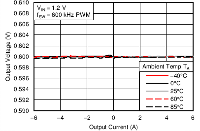
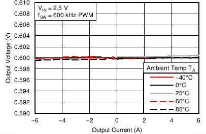
Characterization data tested using the TPS53317EVM-750 where the external tracking input sets the output voltage and operates in non-droop mode. See SLUU642 for detailed configuration.


| VIN = 1.5 V | VOUT = 0.75 V |


| VIN = 1.5 V | VOUT = 0.75 V |