SLUSC39B June 2015 – February 2017 TPS53647
PRODUCTION DATA.
- 1 Features
- 2 Applications
- 3 Description
- 4 Revision History
- 5 Pin Configuration and Functions
- 6 Specifications
-
7 Detailed Description
- 7.1 Overview
- 7.2 Functional Block Diagram
- 7.3
Feature Description
- 7.3.1 V3R3 LDO
- 7.3.2 PWM Operation
- 7.3.3 Current Sense and IMON Calculation
- 7.3.4 Setting the Load-Line (DROOP)
- 7.3.5 Load Transitions
- 7.3.6 Overshoot Reduction (OSR)
- 7.3.7 Undershoot Reduction (USR)
- 7.3.8 AutoBalance™ Current Sharing
- 7.3.9 Phase Overlap
- 7.3.10 VID
- 7.3.11 PWM and SKIP Signals
- 7.3.12 TSEN (Thermal Sense) Pin
- 7.3.13 RESET Function
- 7.3.14 Input UVLO
- 7.3.15 V5 Pin Undervoltage Lockout (UVLO)
- 7.3.16 Output Undervoltage Protection (UVP)
- 7.3.17 Overvoltage Protection (OVP)
- 7.3.18 Overcurrent Limit (OCL) and Overcurrent Protection (OCP)
- 7.3.19 Over Temperature Protection (OTP)
- 7.3.20 VR_HOT and VR_FAULT Indication
- 7.4 Device Functional Modes
- 7.5
Programming
- 7.5.1
User Selections
- 7.5.1.1 Switching Frequency
- 7.5.1.2 IMAX Information
- 7.5.1.3 Boot Voltage
- 7.5.1.4 Per-Phase Overcurrent Limit (OCL) Level
- 7.5.1.5 Overshoot Reduction (OSR) and Undershoot Reduction (USR) Levels
- 7.5.1.6 Slew Rate Selection
- 7.5.1.7 Mode Selections
- 7.5.1.8 Soft Start Slew Rate and PMBus Addresses
- 7.5.1.9 Ramp Selection
- 7.5.1.10 Maximum Active Phase Numbers
- 7.5.1.11 Pinstrap Mode Settings
- 7.5.1.12 NVM Default Settings
- 7.5.1.13 4-Phase Application
- 7.5.2 Supported Protections and Fault Reports
- 7.5.3 Supported PMBus Address and Commands Summary
- 7.5.1
User Selections
- 7.6
Register Maps
- 7.6.1 PMBus Description
- 7.6.2
PMBus Functionality
- 7.6.2.1 PMBus Address
- 7.6.2.2 Pin Strap Settings
- 7.6.2.3
Supported PMBus Commands
- 7.6.2.3.1 OPERATION (01h)
- 7.6.2.3.2 ON_OFF_CONFIG (02h)
- 7.6.2.3.3 CLEAR_FAULTS (03h)
- 7.6.2.3.4 WRITE_PROTECT (10h)
- 7.6.2.3.5 STORE_DEFAULT_ALL (11h)
- 7.6.2.3.6 RESTORE_DEFAULT_ALL (12h)
- 7.6.2.3.7 CAPABILITY (19h)
- 7.6.2.3.8 VOUT_MODE (20h)
- 7.6.2.3.9 VOUT_COMMAND (21h)
- 7.6.2.3.10 VOUT_MAX (24h)
- 7.6.2.3.11 VOUT_MARGIN_HIGH (25h)
- 7.6.2.3.12 VOUT_MARGIN_LOW (26h)
- 7.6.2.3.13 IOUT_CAL_OFFSET (39h)
- 7.6.2.3.14 VOUT_OV_FAULT_RESPONSE (41h)
- 7.6.2.3.15 VOUT_UV_FAULT_RESPONSE (45h)
- 7.6.2.3.16 IOUT_OC_FAULT_LIMIT (46h)
- 7.6.2.3.17 IOUT_OC_FAULT_RESPONSE (47h)
- 7.6.2.3.18 IOUT_OC_WARN_LIMIT (4Ah)
- 7.6.2.3.19 OT_FAULT_LIMIT (4Fh)
- 7.6.2.3.20 OT_FAULT_RESPONSE (50h)
- 7.6.2.3.21 OT_WARN_LIMIT (51h)
- 7.6.2.3.22 VIN_OV_FAULT_LIMIT (55h)
- 7.6.2.3.23 IIN_OC_FAULT_LIMIT (5Bh)
- 7.6.2.3.24 IIN_OC_FAULT_RESPONSE (5Ch)
- 7.6.2.3.25 IIN_OC_WARN_LIMIT (5Dh)
- 7.6.2.3.26 STATUS_BYTE (78h)
- 7.6.2.3.27 STATUS_WORD (79h)
- 7.6.2.3.28 STATUS_VOUT (7Ah)
- 7.6.2.3.29 STATUS_IOUT (7Bh)
- 7.6.2.3.30 STATUS_INPUT (7Ch)
- 7.6.2.3.31 STATUS_TEMPERATURE (7Dh)
- 7.6.2.3.32 STATUS_CML (7Eh)
- 7.6.2.3.33 STATUS_MFR_SPECIFIC (80h)
- 7.6.2.3.34 READ_VIN (88h)
- 7.6.2.3.35 READ_IIN (89h)
- 7.6.2.3.36 READ_VOUT (8Bh)
- 7.6.2.3.37 READ_IOUT (8Ch)
- 7.6.2.3.38 READ_TEMPERATURE_1 (8Dh)
- 7.6.2.3.39 READ_POUT (96h)
- 7.6.2.3.40 READ_PIN (97h)
- 7.6.2.3.41 PMBus_REVISION (98h)
- 7.6.2.3.42 MFR_ID (99h)
- 7.6.2.3.43 MFR_MODEL (9Ah)
- 7.6.2.3.44 MFR_REVISION (9Bh)
- 7.6.2.3.45 MFR_DATE (9Dh)
- 7.6.2.3.46 MFR_VOUT_MIN (A4h)
- 7.6.2.3.47 MFR_SPECIFIC_00 (Per-Phase Overcurrent Limit) (D0h)
- 7.6.2.3.48 MFR_SPECIFIC_01 (Telemetry Averaging Time) (D1h)
- 7.6.2.3.49 MFR_SPECIFIC_04 (Read VOUT) (D4h)
- 7.6.2.3.50 MFR_SPECIFIC_05 (VOUT Trim) (D5h)
- 7.6.2.3.51 MFR_SPECIFIC_07 (Additional Function Bits) (D7h)
- 7.6.2.3.52 MFR_SPECIFIC_08 (Droop) (D8h)
- 7.6.2.3.53 MFR_SPECIFIC_09 (OSR/USR) (D9h)
- 7.6.2.3.54 MFR_SPECIFIC_10 (Maximum Operating Current) (DAh)
- 7.6.2.3.55 MFR_SPECIFIC_11 (VBOOT) (DBh)
- 7.6.2.3.56 MFR_SPECIFIC_12 (Switching Frequency and TRISE) (DCh)
- 7.6.2.3.57 MFR_SPECIFIC_13 (Slew Rate and Other Operation Modes) (DDh)
- 7.6.2.3.58 MFR_SPECIFIC_14 (Ramp Height) (DEh)
- 7.6.2.3.59 MFR_SPECIFIC_15 (Dynamic Phase Shedding Thresholds) (DFh)
- 7.6.2.3.60 MFR_SPECIFIC_16 (VIN UVLO) (E0h)
- 7.6.2.3.61 MFR_SPECIFIC_20 (Maximum Operational Phase Number) (E4h)
- 7.6.2.3.62 MFR_SPECIFIC_22 ( VOUT_UV_FAULT_threshold) (E6h)
- 7.6.2.3.63 MFR_SPECIFIC_44 (DEVICE_CODE) (FCh)
-
8 Application and Implementation
- 8.1 Application Information
- 8.2
Typical Application
- 8.2.1 Design Requirements
- 8.2.2
Detailed Design Procedure
- 8.2.2.1 Select the Switching Frequency
- 8.2.2.2 Set the Maximum Output Current (IMAX)
- 8.2.2.3 Select the Soft-Start Slew Rate
- 8.2.2.4 Select the Operation Mode
- 8.2.2.5 Choose Inductor
- 8.2.2.6 Select the Per-Phase Valley Current Limit And Ramp Level
- 8.2.2.7 Set the Load-Line
- 8.2.2.8 Set the BOOT Voltage
- 8.2.2.9 Set OSR/USR Thresholds to Improve Load Transient Performance
- 8.2.2.10 Digital Current Monitor (IMON) Gain and Filter Setting
- 8.2.2.11 Compensation Design
- 8.2.2.12 Set PMBus Addresses
- 8.2.2.13 Programming the Device with the PMBus
- 8.2.3 Application Curves
- 9 Power Supply Recommendations
-
10Layout
- 10.1
Layout Guidelines
- 10.1.1 Schematic Review Checklist
- 10.1.2
PCB Design Guidelines
- 10.1.2.1 Layer Stack-up, 8-Layer PCB as example
- 10.1.2.2 Current Sensing Lines
- 10.1.2.3 Feedback Voltage Sensing Lines
- 10.1.2.4 PWM Lines
- 10.1.2.5 Power Chain Symmetry
- 10.1.2.6 Placing Analog Signal Components
- 10.1.2.7 Grounding Recommendations
- 10.1.2.8 TI Smart Power Stage CSD95372BQ5MC
- 10.1.2.9 Power Delivery and Power Density
- 10.2 Layout Example
- 10.1
Layout Guidelines
- 11Device and Documentation Support
- 12Mechanical, Packaging, and Orderable Information
Package Options
Mechanical Data (Package|Pins)
- RTA|40
Thermal pad, mechanical data (Package|Pins)
- RTA|40
Orderable Information
8 Application and Implementation
8.1 Application Information
The TPS53647 device has a very simple design procedure. Please contact your local Texas Instruments representative to get a copy of our excel-based design tool spreadsheet. This design describes a typical 4-phase, 1 V, 120 A output application with pinstrap mode.
8.2 Typical Application
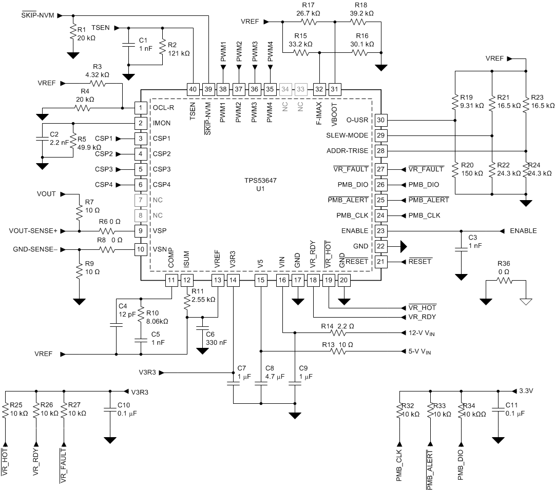 Figure 99. Controller Schematic for a 4-Phase, 1 V, 120 A Application
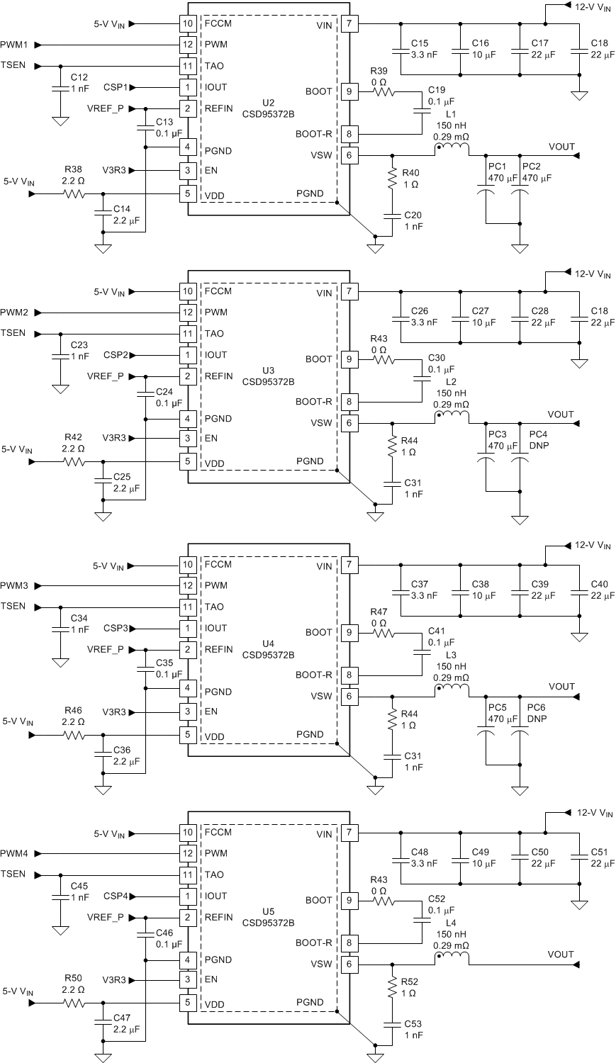 Figure 100. Power Stage Schematic for a 4-Phase, 1V/120A Application
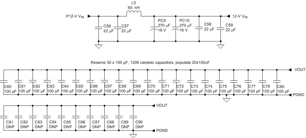 Figure 101. Input and Output Filter for a 4-Phase, 1 V, 120 A Application
8.2.1 Design Requirements
- 4-phase, 1 V, 120 A output
- Number of phases: 4
- Input Voltage 10.8 V – 13.2 V
- Imax: 120 A
- Load-line: Zero Load Line
- Boot voltage, VBOOT: 1.0 V
- PMBus Address: 1110001 (bin)
8.2.2 Detailed Design Procedure
For this design, complete the following steps:
- Select Switching Frequency
- Set the Maximum Output Current
- Select the Soft-Start Slew Rate
- Select the Operation Mode
- Choose Inductor
- Select the Per-Phase Valley Current Limit and Ramp Level
- Set the Load Line
- Set the BOOT Voltage
- Set OSR/USR Thresholds for Improving Load Transient Performance
- Determine Digital Current Monitor (IMON) Gain and Filter Setting
- Adjust Compensation Design
- Set the PMBus Addresses
- Program the Device with the PMBus
8.2.2.1 Select the Switching Frequency
The value of a resistor (RF) between the F-IMAX pin and GND selects the switching frequency. The frequency is an approximate frequency and is expected to vary based on load and input voltage.
Table 72. Frequency Selection Table
| SELECTION RESISTOR (RF) VALUE (kΩ) |
OPERATING FREQUENCY (fSW) (kHz) |
|---|---|
| 20 | 300 |
| 24 | 400 |
| 30 | 500 |
| 39 | 600 |
| 56 | 700 |
| 75 | 800 |
| 100 | 900 |
| 150 | 1000 |
For this design, choose 500 kHz for the switching frequency. So, RF = 30 kΩ.
8.2.2.2 Set the Maximum Output Current (IMAX)
The voltage on the F-IMAX pin sets the maximum output current from the value of the resistors connected from the VREF pin to the F-IMAX pin (RIMAX). Equation 7 shows the maximum output current calculation.
NOTE
The default total overcurrent threshold is 125% of IMAX

Use Equation 8 to calculate RIMAX.

From Table 72, RF = 30 kΩ. Selecting the closest standard resistor value, RIMAX = 33.2 kΩ
NOTE
The tolerance of the RF and RIMAX resistors affect IIMAX value. If the design requires an accurate IIMAX is needed, select an RF and an RIMAX value with tight tolerance (0.5% or 0.1%).
8.2.2.3 Select the Soft-Start Slew Rate
To select the soft-start slew rate, the first step is to select the output voltage change slew rate. The resistor (RSLEW) (connected between the SLEW-MODE pin and GND) sets the output voltage change slew rate when using VOUT_COMMAND. Table 73 show a summary of these settings. For a minimum 0.68-mV/μs slew rate, the resistor RSLEW = 24.3 kΩ.
Table 73. Vout Change Slew Rate Selection
| SELECTION RESISTOR RSLEW (kΩ) |
MINIMUM SLEW RATE ( mV/µs) |
|---|---|
| 20 | 0.34 |
| 24 | 0.68 |
| 30 | 1.02 |
| 39 | 1.36 |
| 56 | 1.7 |
| 75 | 2.04 |
| 100 | 2.38 |
| 150 | 2.74 |
After determining the VOUT change slew rate, select the ratio of soft-start rate versus VOUT change slew rate. Select a value for resistor RADDR (the resistor between ADDR_TRISE pin and GND) to configure this ratio.
Table 74. Soft-Start Slew Rate Selection
| SELECTION RESISTOR RADDR (kΩ) |
MINIMUM SLEW RATE ( mV/µs) |
|---|---|
| 20 or 24 | 1 |
| 30 or 39 | 1/2 |
| 56 or 75 | 1/4 |
| 100 or 150 | 1/8 |
In this design, the soft-start slew rate is the same as Vout change slew rate. So RADDR=20k or 24k is selected. The LSB of BOOT voltage VID determines the value of RADDR as described in Set the BOOT Voltage. If slower soft start is desired, higher RADDR can be used to set soft-start slew rate to be 1/2, 1/4 or 1/8 of output voltage change slew rate.
8.2.2.4 Select the Operation Mode
The resistor (RMODE) is connected between the VREF pin and the SLEW-MODE pin. After selecting the value of RSLEW, set the operation mode by choosing the voltage on the SLEW-MODE pin as summarized in Table 75 and the Electrical Characteristics table. In this design, VR 12.0 mode is selected with 4-phase interleaving, disabled dynamic phase shedding, and zero load-line. As described in the Select the Soft-Start Slew Rate section, use the value RSLEW = 24 kΩ, so RMODE = 16.5 kΩ to select the desired operating modes.
Table 75. Operation Mode with Resistor Selection
| OPERATION MODES BIT | BIT DESCRIPTION | ||
|---|---|---|---|
| Mode bit M3 | MFR_SPEC_13<7> | VR12MODE | 0: VR12.5 (Use VR12.5 VID table) |
| 1: VR12.0 (Use VR12.0 VID table) | |||
| Mode bit M2 | MFR_SPEC_13<6> | PISET | 0: 4 phase interleaving individually |
| 1: 1/3 and 2/4 phase interleaving | |||
| Mode bit M1 | MFR_SPEC_13<4> | DPSEN | 0: Disable dynamic phase shedding |
| 1: Enable dynamic phase shedding | |||
| Mode bit M0 | MFR_SPEC_13<3> | ZLLSET | 0: Non-zero load-line |
| 1: Zero load-line | |||
8.2.2.5 Choose Inductor
Smaller inductance values yield better transient performance, but also have a higher ripple and lower efficiency. Higher inductance values have the opposite characteristics. It is common practice to limit the ripple current to between 20% and 50% of the maximum per-phase current. In this design example, 40% of the maximum per-phase current is used.


The inductor with a value of 150 nH and saturation current of ISAT = 61 A at 100°C is selected for this application. This saturation current level can be used to determine the OCL level. So the IOCL is selected to be 48 A to use in the OCL resistor calculation in Equation 11.

8.2.2.6 Select the Per-Phase Valley Current Limit And Ramp Level
The per-phase, valley current limit is selected by the resistor (ROCL) from OCL-R pin to GND as shown in Table 76. The RAMP is set by the voltage on OCL_R pin with resistor (RRAMP) from OCL_R pin to VREF. The current limit is selected so that the output current OCL is higher than the maximum per-phase current to allow sufficient room for current increase during load transient while the peak inductor current is still lower saturation current level.
Table 76. Per-Phase Valley Current Limit vs Resistor Selection
| VOCL(V) | ROCL-R (kΩ) | PER-PHASE VALLEY CURRENT LIMIT (A) |
|---|---|---|
| ≤ 0.85 | 20 | 24 |
| 24 | 27 | |
| 30 | 30 | |
| 39 | 33 | |
| 56 | 36 | |
| 75 | 39 | |
| 100 | 42 | |
| 150 | 45 | |
| ≥ 0.95 | 20 | 48 |
| 24 | 51 | |
| 30 | 54 | |
| 39 | 57 | |
| 56 | 60 | |
| 75 | 63 | |
| 100 | 66 | |
| 150 | 69 |
Table 77. Ramp Level vs OCL_R Pin Voltage Selection
| VOCL-R (V) | RAMP LEVEL ( mVp-p) |
|---|---|
| 0.2 ±50 mV or 1.0 ±50 mV | 40 |
| 0.4 ±50 mV or 1.2 ±50 mV | 80 |
| 0.6 ±50 mV or 1.4 ±50 mV | 150 |
| 0.8 ±50mV or 1.6 ±50mV | 200 |
In this design example, a 48-A valley current limit is selected, so ROCL is chosen as 20 kΩ.
In this example, a ramp voltage of 150 mV is chosen. The user may chose a lower ramp value to improve transient performance if jitter performance is less of a concern. This value depends on the board layout and individual layout requirements.
Table 76 notes that VOCL must be ≥ 1.0 V. Table 77 shows that for a 150- mV ramp, VOCL must be 1.4 V, therefore the value of the resistor placed between the OCL-R pin and the VREF pin (ROCL-R) should be 4.32 kΩ.
8.2.2.7 Set the Load-Line
The load-line is set by the resistor, RISUM, from ISUM pin to VREF. Please note a 0 Ω resistor will be used since load line setting is not required for this design example.
The below procedure is provided for applications when a 1.05 mΩ load line is needed.

where
- RLL is the desired load-line
- gM(isum) is the ISUM amplifier transconductance
- RCS is the current-sensing gain from the CSD95372B
- ACS is the internal gain
Because the sensed current from the CSD95372B device is temperature-compensated, a NTC network is not required to achieve a simple application circuit.
8.2.2.8 Set the BOOT Voltage
The resistor, RBOOT, placed between the VBOOT pin and GND as shown in Table 78 sets bit 3, 2, and 1 of the VID of the BOOT voltage. The voltage on VBOOT pin sets bit 7, 6, 5, 4 of the VID of the BOOT voltage. The resistor between the ADDR_TRISE pin and GND sets bit 0 of VID of the BOOT voltage. The BOOT voltage selection also depends on the operation mode selected in the Select the Operation Mode section. In this design example, 1.0 V is selected as the BOOT voltage in VR12.0 mode, and the VID is 1001 0111, so the RBOOT = 39 kΩ, VVBOOT = 1.009 V, RADDR= 24 kΩ.
Table 78. Boot Voltage VID Selection (Step 1)
| RBOOT (kΩ) | BOOT VOLTAGE VID |
|
|---|---|---|
| B3B2B1 | ||
| 20 | 000 | |
| 24 | 001 | |
| 30 | 010 | |
| 39 | 011 | |
| 56 | 100 | |
| 75 | 101 | |
| 100 | 110 | |
| 150 | 111 | |
Table 79. Boot Voltage VID Selection (Step 2)
Table 80. Boot Voltage VID Selection (Step 3)
| RADDR (kΩ) | BOOT VOLTAGE VID | |||
|---|---|---|---|---|
| B0 | ||||
| 20 or 30 or 56 or 100 | 0 | |||
| 24 or 39 or 75 or 150 | 1 | |||
8.2.2.9 Set OSR/USR Thresholds to Improve Load Transient Performance
The resistor, ROSR connected between the O-USR pin and GND as shown in Table 81 sets the overshoot reduction (OSR) threshold.
Table 81. OSR Threshold vs Resistor Selection
| RO-USR
(kΩ) |
OSR THRESHOLD ( mV) |
|---|---|
| 20 | 30 |
| 24 | 40 |
| 30 | 60 |
| 39 | 80 |
| 56 | 100 |
| 75 | 120 |
| 100 | 140 |
| 150 | OFF |
The required OSR setting is based on the load-transient performance and the amount of the actual output capacitance. The suggested method is to start with OSR OFF and perform the load transient per the application requirement. If the overshoot can meet the specification with the chosen output capacitance, then the OSR can be kept OFF. So the resistor ROSR can be selected as 150 kΩ. Otherwise the OSR threshold can be lowered by choosing a lower setting from the Table 81 to reduce the overshoot to meet the specifications.
Once ROSR is selected, the Undershoot Reduction (USR) threshold is set by the voltage on the O-USR pin with the resistor, RUSR, from the O-USR pin to VREF as shown in Table 82.
Table 82. USR Threshold vs Voltage Selection
The design procedure for the USR threshold is similar to the OSR setting. The initial setting of the USR threshold is to start with USR OFF, and then perform the load transient test. If the undershoot can meet the requirement, the USR setting can remain OFF. In this design the USR setting is OFF.
8.2.2.10 Digital Current Monitor (IMON) Gain and Filter Setting
To correctly monitor digital current values, the gain of the analog current monitor should be determined by setting the IMON voltage to 0.85 V for maximum output current IMAX. When PMBus host sends the READ_IOUT command, the current information is reported.
RIMON can be determined by using Equation 13

where
- RIMON is the desired impedance on the IMON pin
- IMAX is the total maximum output current
- RCS is the current sense gain from CSD95372B
- SF is is the internal current gain scaling factor
In this design example, IMAX = 120 A, so the resistance, RIMON, is calculated as 49.58 kΩ. Use the standard value of 49.99kΩ. A capacitor, CIMON usually connected in parallel with RIMON to provide filtering on the IMON signal. In this design, a CIMON value of 2.2 nF is selected.
8.2.2.11 Compensation Design
A type-II compensator is used with the DCAP+ architecture of TPS53647 as shown in Figure 102. gM(comp) is the COMP amplifier transconductance, which is typically 0.5 mS. RCOMP determines the gain and the compensation pole and zero locations. CCOMPS determines the compensation zero to increase the phase margin, and CCOMPP determines the compensation pole to filter out the high-frequency noise. The actual compensator design needs to be adjusted, based on the experimental test results and the bode plot measurements. In this example, RCOMP = 8.06 kΩ, CCOMPS = 1 nF, and CCOMPP = 12 pF to put the compensation zero at 19.7 kHz and the compensator pole at 1.65 MHz.
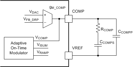 Figure 102. Compensation Circuitry
8.2.2.12 Set PMBus Addresses
To communicate with system controllers or host with PMBus interfaces, the slave address of the TPS53647 device needs to be set. The voltage on ADDR_TRISE pin sets the PMBus address. Since the resistance of RADDR is already determined (24 kΩ), The resistance between ADDR_TRISE pin and VREF can be calculated. In this design, PMBUs address of 111 0001 is used. The resistor between ADDR_TRISE and VREF is 16.5 kΩ.
8.2.2.13 Programming the Device with the PMBus
It is optional to use the PMBus interface to program the TPS53647 device since all the settings can be configured externally by using resistors; however, the system controller can override the configurations or can program the device to change the operation modes using the PMBus. The supported PMBus command sets have been introduced in the previous section for the firmware development.
8.2.3 Application Curves
4-Phase, 120-A, full load application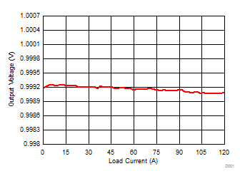
| VIN = 12.0 V | VV5 = 5.0 V |
| VOUT = 1.0 V | Loadline = 0 mΩ |
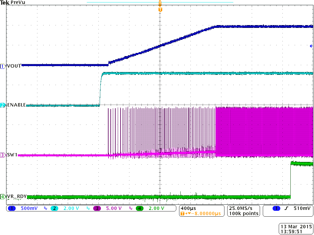
| VIN = 12 V | VOUT = 1.0 V | IOUT = 0 A |
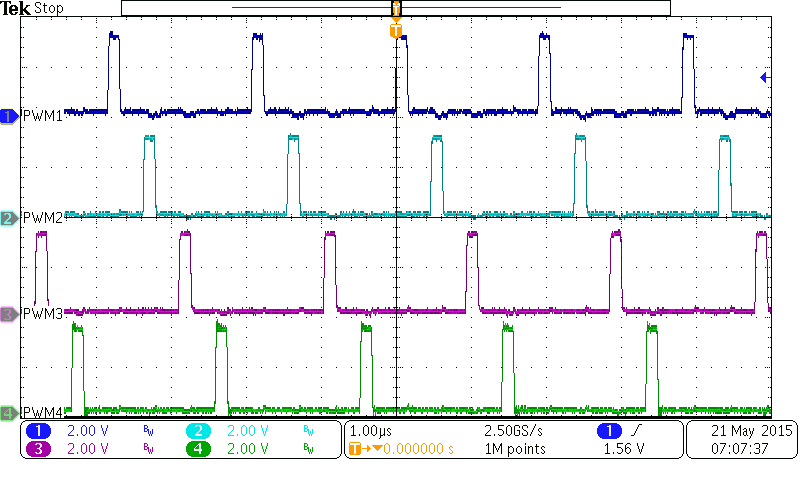
| VIN = 12 V | VOUT = 1.0 V | IOUT= 90 A |
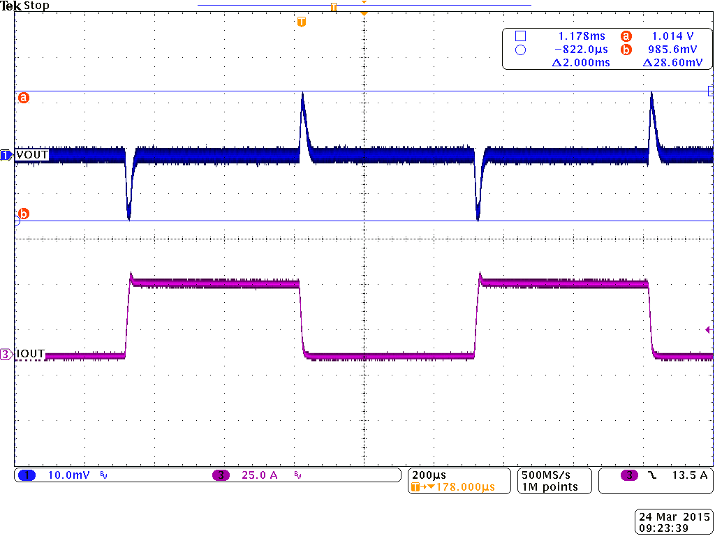
| VVIN = 12 V | VOUT = 1.0 V |
| 30-A Load Step |
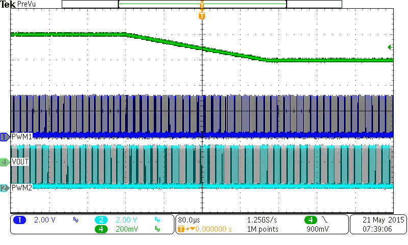
| VIN = 12 V | IOUT = 9 A |
| VBOOT=1.0 V | VOUT COMMAND change to 0.8 V |
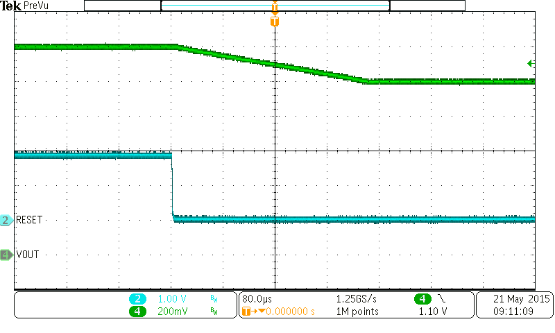
| VIN = 12 V | IOUT = 9 A |
| VBOOT=1.0 V | VOUT = 1.2 V |
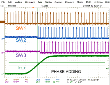 Figure 115. Phase Adding
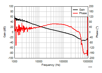
| 6-Phase Operation | VIN = 12 V | ||
| VOUT = 1.0 V | IOUT = 180 A |
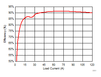
| VIN = 12.0 V | VV5 = 5.0 V |
| VOUT = 1.0 V | fSW = 500 kHz |
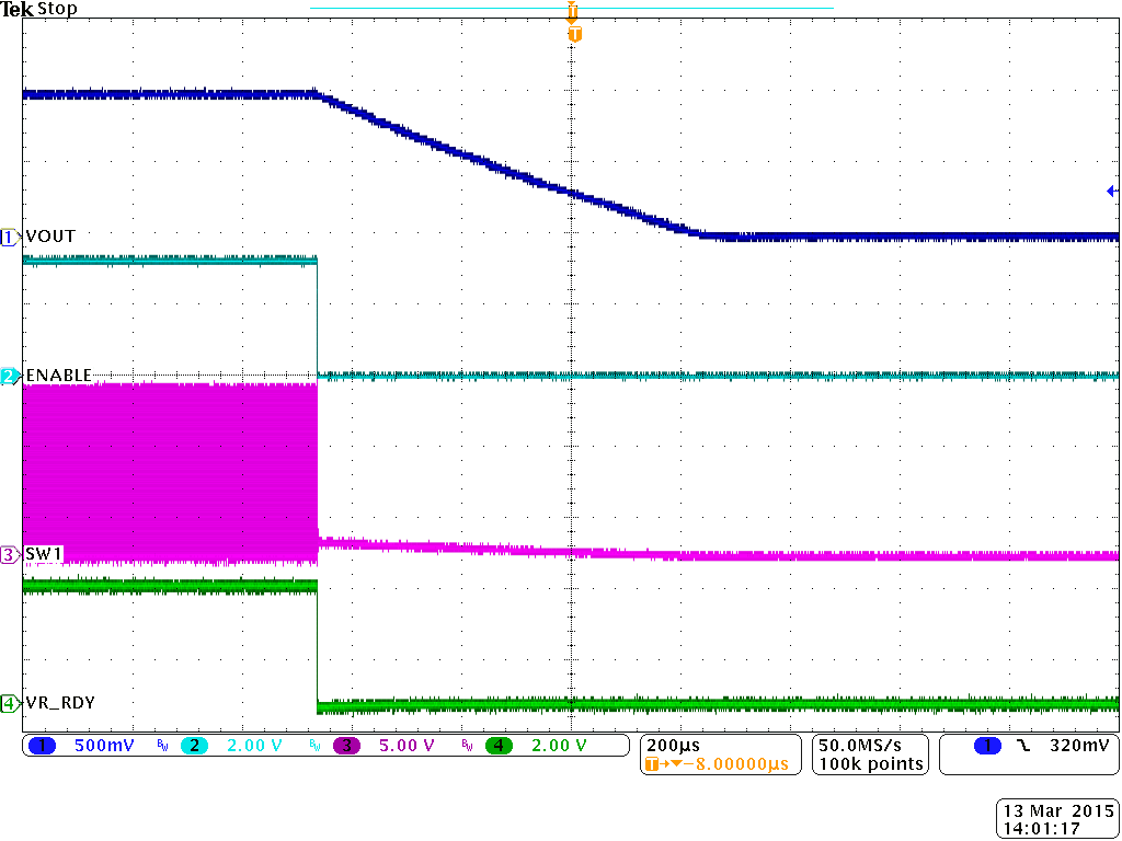
| VIN = 12 V | VOUT = 1.0 V | IOUT = 9 A |
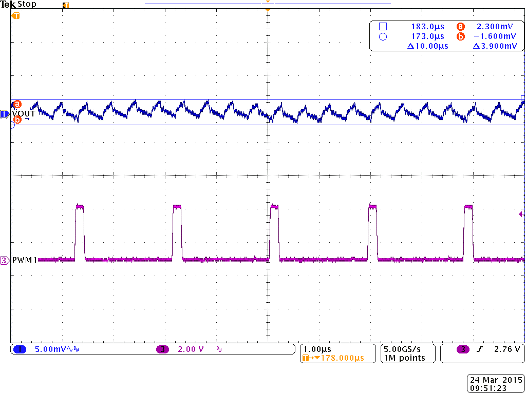
| VIN = 12 V | VOUT = 1.0 V | IOUT = 180 A |
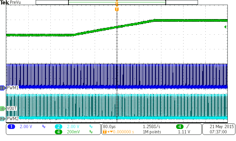
| VIN = 12 V | IOUT = 9 A |
| VBOOT=1.0 V | VOUT COMMAND change to 1.2 V |
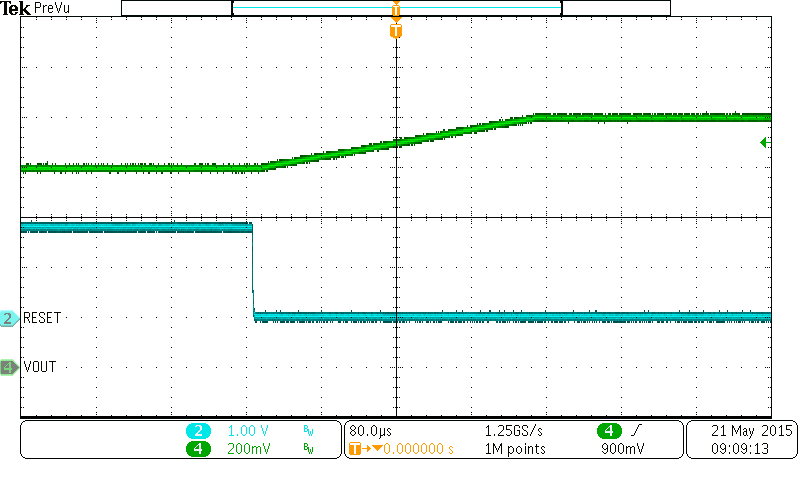
| VIN = 12 V | IOUT = 9 A |
| VBOOT=1.0 V | VOUT = 0.8 V |
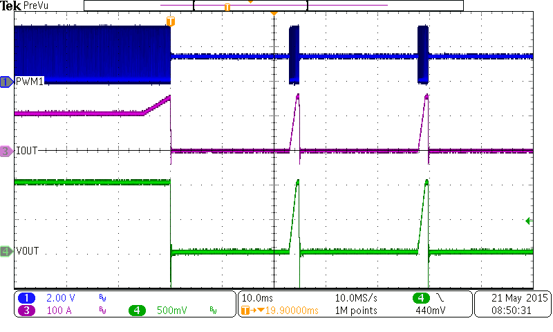
| VIN = 12 V | VOUT = 1.0 V |
| OC_FAULT_LIMIT=200 A | IOUT = 205 A |
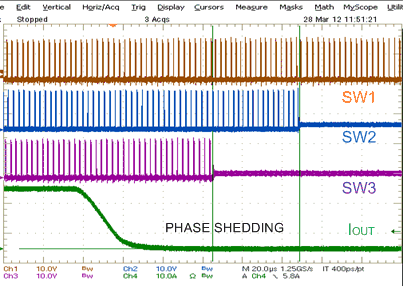 Figure 116. Phase Shedding