SLUSC39B June 2015 – February 2017 TPS53647
PRODUCTION DATA.
- 1 Features
- 2 Applications
- 3 Description
- 4 Revision History
- 5 Pin Configuration and Functions
- 6 Specifications
-
7 Detailed Description
- 7.1 Overview
- 7.2 Functional Block Diagram
- 7.3
Feature Description
- 7.3.1 V3R3 LDO
- 7.3.2 PWM Operation
- 7.3.3 Current Sense and IMON Calculation
- 7.3.4 Setting the Load-Line (DROOP)
- 7.3.5 Load Transitions
- 7.3.6 Overshoot Reduction (OSR)
- 7.3.7 Undershoot Reduction (USR)
- 7.3.8 AutoBalance™ Current Sharing
- 7.3.9 Phase Overlap
- 7.3.10 VID
- 7.3.11 PWM and SKIP Signals
- 7.3.12 TSEN (Thermal Sense) Pin
- 7.3.13 RESET Function
- 7.3.14 Input UVLO
- 7.3.15 V5 Pin Undervoltage Lockout (UVLO)
- 7.3.16 Output Undervoltage Protection (UVP)
- 7.3.17 Overvoltage Protection (OVP)
- 7.3.18 Overcurrent Limit (OCL) and Overcurrent Protection (OCP)
- 7.3.19 Over Temperature Protection (OTP)
- 7.3.20 VR_HOT and VR_FAULT Indication
- 7.4 Device Functional Modes
- 7.5
Programming
- 7.5.1
User Selections
- 7.5.1.1 Switching Frequency
- 7.5.1.2 IMAX Information
- 7.5.1.3 Boot Voltage
- 7.5.1.4 Per-Phase Overcurrent Limit (OCL) Level
- 7.5.1.5 Overshoot Reduction (OSR) and Undershoot Reduction (USR) Levels
- 7.5.1.6 Slew Rate Selection
- 7.5.1.7 Mode Selections
- 7.5.1.8 Soft Start Slew Rate and PMBus Addresses
- 7.5.1.9 Ramp Selection
- 7.5.1.10 Maximum Active Phase Numbers
- 7.5.1.11 Pinstrap Mode Settings
- 7.5.1.12 NVM Default Settings
- 7.5.1.13 4-Phase Application
- 7.5.2 Supported Protections and Fault Reports
- 7.5.3 Supported PMBus Address and Commands Summary
- 7.5.1
User Selections
- 7.6
Register Maps
- 7.6.1 PMBus Description
- 7.6.2
PMBus Functionality
- 7.6.2.1 PMBus Address
- 7.6.2.2 Pin Strap Settings
- 7.6.2.3
Supported PMBus Commands
- 7.6.2.3.1 OPERATION (01h)
- 7.6.2.3.2 ON_OFF_CONFIG (02h)
- 7.6.2.3.3 CLEAR_FAULTS (03h)
- 7.6.2.3.4 WRITE_PROTECT (10h)
- 7.6.2.3.5 STORE_DEFAULT_ALL (11h)
- 7.6.2.3.6 RESTORE_DEFAULT_ALL (12h)
- 7.6.2.3.7 CAPABILITY (19h)
- 7.6.2.3.8 VOUT_MODE (20h)
- 7.6.2.3.9 VOUT_COMMAND (21h)
- 7.6.2.3.10 VOUT_MAX (24h)
- 7.6.2.3.11 VOUT_MARGIN_HIGH (25h)
- 7.6.2.3.12 VOUT_MARGIN_LOW (26h)
- 7.6.2.3.13 IOUT_CAL_OFFSET (39h)
- 7.6.2.3.14 VOUT_OV_FAULT_RESPONSE (41h)
- 7.6.2.3.15 VOUT_UV_FAULT_RESPONSE (45h)
- 7.6.2.3.16 IOUT_OC_FAULT_LIMIT (46h)
- 7.6.2.3.17 IOUT_OC_FAULT_RESPONSE (47h)
- 7.6.2.3.18 IOUT_OC_WARN_LIMIT (4Ah)
- 7.6.2.3.19 OT_FAULT_LIMIT (4Fh)
- 7.6.2.3.20 OT_FAULT_RESPONSE (50h)
- 7.6.2.3.21 OT_WARN_LIMIT (51h)
- 7.6.2.3.22 VIN_OV_FAULT_LIMIT (55h)
- 7.6.2.3.23 IIN_OC_FAULT_LIMIT (5Bh)
- 7.6.2.3.24 IIN_OC_FAULT_RESPONSE (5Ch)
- 7.6.2.3.25 IIN_OC_WARN_LIMIT (5Dh)
- 7.6.2.3.26 STATUS_BYTE (78h)
- 7.6.2.3.27 STATUS_WORD (79h)
- 7.6.2.3.28 STATUS_VOUT (7Ah)
- 7.6.2.3.29 STATUS_IOUT (7Bh)
- 7.6.2.3.30 STATUS_INPUT (7Ch)
- 7.6.2.3.31 STATUS_TEMPERATURE (7Dh)
- 7.6.2.3.32 STATUS_CML (7Eh)
- 7.6.2.3.33 STATUS_MFR_SPECIFIC (80h)
- 7.6.2.3.34 READ_VIN (88h)
- 7.6.2.3.35 READ_IIN (89h)
- 7.6.2.3.36 READ_VOUT (8Bh)
- 7.6.2.3.37 READ_IOUT (8Ch)
- 7.6.2.3.38 READ_TEMPERATURE_1 (8Dh)
- 7.6.2.3.39 READ_POUT (96h)
- 7.6.2.3.40 READ_PIN (97h)
- 7.6.2.3.41 PMBus_REVISION (98h)
- 7.6.2.3.42 MFR_ID (99h)
- 7.6.2.3.43 MFR_MODEL (9Ah)
- 7.6.2.3.44 MFR_REVISION (9Bh)
- 7.6.2.3.45 MFR_DATE (9Dh)
- 7.6.2.3.46 MFR_VOUT_MIN (A4h)
- 7.6.2.3.47 MFR_SPECIFIC_00 (Per-Phase Overcurrent Limit) (D0h)
- 7.6.2.3.48 MFR_SPECIFIC_01 (Telemetry Averaging Time) (D1h)
- 7.6.2.3.49 MFR_SPECIFIC_04 (Read VOUT) (D4h)
- 7.6.2.3.50 MFR_SPECIFIC_05 (VOUT Trim) (D5h)
- 7.6.2.3.51 MFR_SPECIFIC_07 (Additional Function Bits) (D7h)
- 7.6.2.3.52 MFR_SPECIFIC_08 (Droop) (D8h)
- 7.6.2.3.53 MFR_SPECIFIC_09 (OSR/USR) (D9h)
- 7.6.2.3.54 MFR_SPECIFIC_10 (Maximum Operating Current) (DAh)
- 7.6.2.3.55 MFR_SPECIFIC_11 (VBOOT) (DBh)
- 7.6.2.3.56 MFR_SPECIFIC_12 (Switching Frequency and TRISE) (DCh)
- 7.6.2.3.57 MFR_SPECIFIC_13 (Slew Rate and Other Operation Modes) (DDh)
- 7.6.2.3.58 MFR_SPECIFIC_14 (Ramp Height) (DEh)
- 7.6.2.3.59 MFR_SPECIFIC_15 (Dynamic Phase Shedding Thresholds) (DFh)
- 7.6.2.3.60 MFR_SPECIFIC_16 (VIN UVLO) (E0h)
- 7.6.2.3.61 MFR_SPECIFIC_20 (Maximum Operational Phase Number) (E4h)
- 7.6.2.3.62 MFR_SPECIFIC_22 ( VOUT_UV_FAULT_threshold) (E6h)
- 7.6.2.3.63 MFR_SPECIFIC_44 (DEVICE_CODE) (FCh)
-
8 Application and Implementation
- 8.1 Application Information
- 8.2
Typical Application
- 8.2.1 Design Requirements
- 8.2.2
Detailed Design Procedure
- 8.2.2.1 Select the Switching Frequency
- 8.2.2.2 Set the Maximum Output Current (IMAX)
- 8.2.2.3 Select the Soft-Start Slew Rate
- 8.2.2.4 Select the Operation Mode
- 8.2.2.5 Choose Inductor
- 8.2.2.6 Select the Per-Phase Valley Current Limit And Ramp Level
- 8.2.2.7 Set the Load-Line
- 8.2.2.8 Set the BOOT Voltage
- 8.2.2.9 Set OSR/USR Thresholds to Improve Load Transient Performance
- 8.2.2.10 Digital Current Monitor (IMON) Gain and Filter Setting
- 8.2.2.11 Compensation Design
- 8.2.2.12 Set PMBus Addresses
- 8.2.2.13 Programming the Device with the PMBus
- 8.2.3 Application Curves
- 9 Power Supply Recommendations
-
10Layout
- 10.1
Layout Guidelines
- 10.1.1 Schematic Review Checklist
- 10.1.2
PCB Design Guidelines
- 10.1.2.1 Layer Stack-up, 8-Layer PCB as example
- 10.1.2.2 Current Sensing Lines
- 10.1.2.3 Feedback Voltage Sensing Lines
- 10.1.2.4 PWM Lines
- 10.1.2.5 Power Chain Symmetry
- 10.1.2.6 Placing Analog Signal Components
- 10.1.2.7 Grounding Recommendations
- 10.1.2.8 TI Smart Power Stage CSD95372BQ5MC
- 10.1.2.9 Power Delivery and Power Density
- 10.2 Layout Example
- 10.1
Layout Guidelines
- 11Device and Documentation Support
- 12Mechanical, Packaging, and Orderable Information
Package Options
Mechanical Data (Package|Pins)
- RTA|40
Thermal pad, mechanical data (Package|Pins)
- RTA|40
Orderable Information
10 Layout
10.1 Layout Guidelines
10.1.1 Schematic Review Checklist
- Confirm the pin-out of the controller on schematic to the pin-out of datasheet
- Get a closest TI reference design to check for connection and component values
- Have a component value design tool ready to check component values.
- Carefully confirm the choice of inductor and DCR (see the Detailed Design Procedure section).
- Carefully confirm the choice of output capacitors (see the Detailed Design Procedure section).
- Confirm the polarity of the differential pair of voltage sensing (VSP/VSN).
- Confirm the current sensing feedback and reference voltage of TI smart power stages (ex: CSD95372BQ5MC).
- A separated IC ground (analog ground) is recommended but not a must.
10.1.2 PCB Design Guidelines
MOST CRITICAL LAYOUT REQUIREMENT
Separate noisy driver interface lines from sensitive analog lines.
The TPS53647 device makes this separation easy. The power stage (CSD95372B) is outside of the TPS53647 device. So all gate-drive and switch-node traces must be local to the inductor and the MOSFETs.
10.1.2.1 Layer Stack-up, 8-Layer PCB as example
- Top Layer: VIN, VOUT, power ground and analog ground
- Layer 2: Power ground
- Layer 3: VIN, VREF, VOUT, PWM signals, and current sense signals
- Layer 4: Power ground, analog ground, and VOUT plane
- Layer5: Power ground, V3R3, and VOUT plane
- Layer 6: V5, VIN and VOUT plane
- Layer 7: Power ground
- Bottom Layer: VIN, VOUT, power ground, analog ground, and feedbacks
10.1.2.2 Current Sensing Lines
Given the physical layout of most systems, the current feedback (CSPx) may have to pass near the power chain. Clean current feedback is required for good load-line, current sharing, and current limiting performance of the TPS53647, so please take the following precautions:
- Run the current feedback signals in the VREF plane as shown in Figure 119.
- Recommended trace width is 8-10 mil
- The distance of each trace should be larger than 20 mil
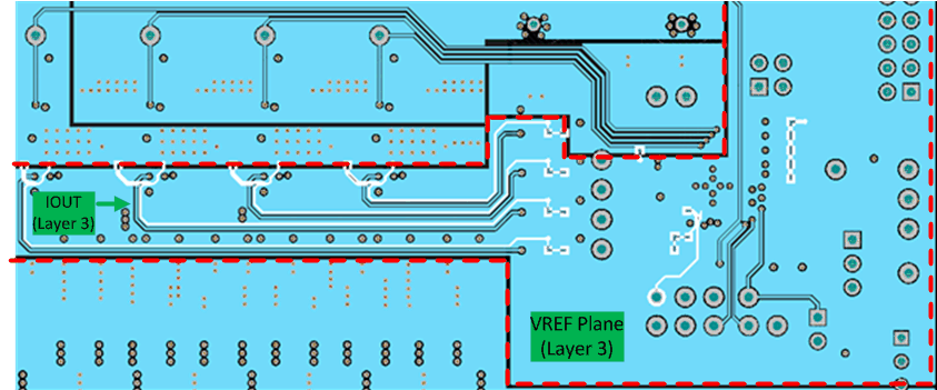 Figure 119. Layout Example of Current Sensing Traces
10.1.2.3 Feedback Voltage Sensing Lines
The voltage feedback coming from the load must be routed as differential pair (distance ≤ 10 mil) all the way to the TPS53647 VSP and VSN pins. Recommended trace width is 8-10 mil. Care should be taken to avoid routing over switch-node traces.
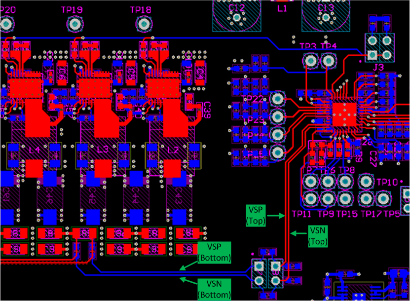 Figure 120. Layout Example for Feedback Voltage Sensing Traces
10.1.2.4 PWM Lines
The PWM lines should be routed from the (TPS53647) device to the power stage (CSD95372B) without crossing any switch-node signals.
 Figure 121. Layout Example for PWM Traces
10.1.2.5 Power Chain Symmetry
The TPS53647 device does not require special care in the layout of the power chain components. This is because independent isolated current feedback is provided. If it is possible to lay out the phases in a symmetrical manner, then please do so. The rule is: the current feedback from each phase needs to be clean of noise and have the same effective current sense resistance.
10.1.2.6 Placing Analog Signal Components
Place components close to the TPS53647 device in the following order, as shown in Figure 122:
- COMP pin and ISUM pin compensation components must be put on the same side of the controller as shown in. Recommended trace width is 8-10 mil.
- Decoupling capacitors for VREF, V3R3, and V5 must be put on the same side of the controller as shown in. Recommended trace width is 8-10 mil.
- Decouple VREF to GND with at most 0.47-uF ceramic capacitor.
- Decouple V3R3 to GND with at least 1-uF ceramic capacitor.
- Decouple V5 to GND with at least 4.7-uF ceramic capacitor. A 1-Ω resistor between 5V supply voltage and V5 pin is also recommended as a filter.
- Decouple VIN to GND with at least 1-uF ceramic capacitor. A 1-Ω resistor between 12V supply voltage and VIN pin is also recommended as a filter.
- OCL-R resistors, F-IMAX resistors, SLEW-MODE resistors, VBOOT resistors, IMON resistor, and O-USR resistors. Recommended trace width is 8-10 mil.
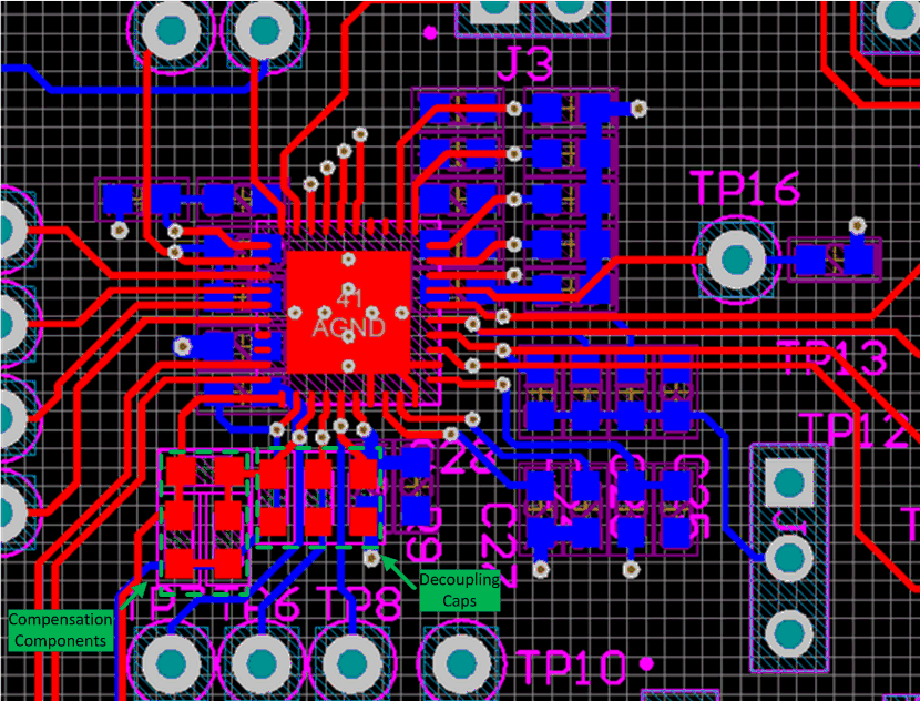 Figure 122. Layout Example of Decoupling Caps and Compensation Components
10.1.2.7 Grounding Recommendations
The TPS53647 device has a GND pin, and a thermal pad. The normal procedure for connecting these follows:
- The thermal pad does not have an electrical connection to the TPS53647 device. However, it is suggested to be connected to GND pin of the TPS53647 device (analog ground) to give good ground shielding as shown in Figure 123
- All the analog components should connect to this analog ground island
- Use a single point connection from analog ground to the power ground.
- The return path of the decoupling capacitors (V3R3, V5, VREF, Vin) should be as short as possible.
- When a separated analog ground is used, it's recommended to have an analog ground shape in layer 3 (assuming controller is on the top layer) to interconnect all the analog ground signals.
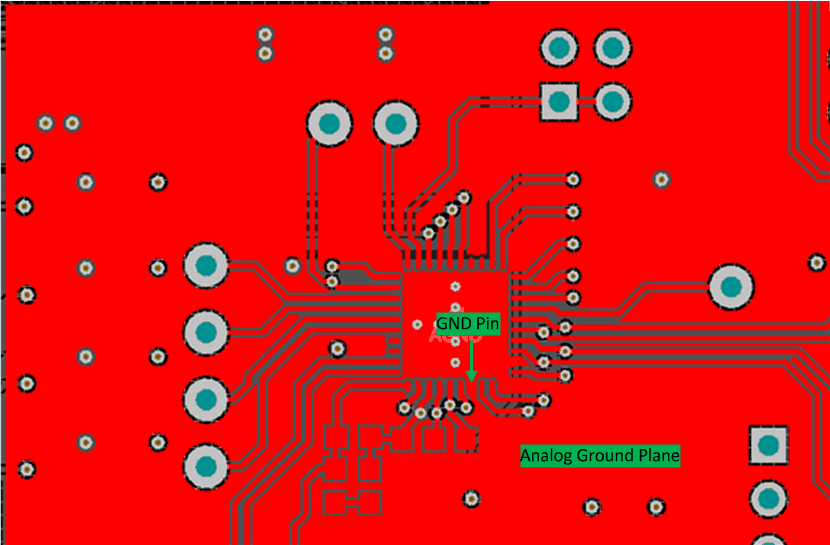 Figure 123. Layout Example for TPS53647 Grounding
10.1.2.8 TI Smart Power Stage CSD95372BQ5MC
The following layout recommendations refer to the CSD95372BQ5MC. Download the datasheet (SLPS417) for more details.
10.1.2.8.1 Electrical Performance
The CSD95372BQ5MC has the ability to switch at voltage rates greater than 10 kV/µs. Special care must be taken with the PCB layout design and placement of the input capacitors, inductor and output capacitors.
- The placement of the input capacitors relative to VIN and PGND pins of CSD95372BQ5MC device should have the highest priority during the component placement routine. It is critical to minimize these node lengths. As such, place ceramic input capacitors as close as possible to the VIN and PGND pins. The example in uses 1 × 3300 pF, 0402, 50-V, X7R ceramic capacitor and 3 × 22 µF, 1206, 25-V ceramic capacitors (TDK part number C3216X5R1E226M160AB or equivalent). Notice there are ceramic capacitors on both sides of the board with an appropriate amount of vias interconnecting both layers.
- Closely connect the bootstrap capacitor (0.1-µF, 0603, 25-V ceramic capacitor) between the BOOT and BOOT_R pins.
- The switching node of the output inductor should be placed relatively close to the Power Stage CSD95372BQ5MC VSW pins. Minimizing the VSW node length between these two components reduces the PCB conduction losses and actually reduce the switching noise level.
10.1.2.8.2 Thermal Performance
The CSD95372BQ5MC has the ability to use the GND planes as the primary thermal path. As such, the use of thermal vias is an effective way to pull away heat from the device and into the system board. Concerns of solder voids and manufacturability problems can be addressed by the use of three basic tactics to minimize the amount of solder attach that will wick down the via barrel:
- Intentionally space out the vias from each other to avoid a cluster of holes in a given area.
- Use the smallest drill size allowed in your design. The example in uses vias with a 12 mil drill hole and a 26 mil capture pad.
- Tent the opposite side of the vias with solder-mask.
In the end, the number and drill size of the thermal vias should align with the end user’s PCB design rules and manufacturing capabilities.
10.1.2.8.3 Sensing Performance
The thermal sensing output TAO pin must be properly decoupled for accurate reporting. As discussed above, a 1nF 25V X7R ceramic capacitor should be placed between TAO and PGND as close to the TAO pin as practical.
The integrated current sensing technology built into the driver of the CSD95372BQ5MC produces an analog signal that is proportional to the inductor current with a proportionality constant of 5 mV/A. This signal is referenced to the voltage applied to REFIN. For optimal performance of this technology a 0.1µF or larger ceramic capacitor should be placed across the REFIN and PGND pins as close as possible to the device.
In addition the IOUT pin should be routed back to the TPS53647 device in a quiet inner layer. If multiple CSD95372BQ5M’s are used on the same board, the IOUT traces should have at least 20 mils spacing between them. Capacitive loading of the IOUT pin should be avoided to maintain the integrity of the sensed signal.
10.1.2.9 Power Delivery and Power Density
Power stage layout guidelines:
- Maximize the widths of power, ground and drive signal connections.
- For conductors in the power path, be sure there is adequate trace width for the amount of current flowing through the traces.
- Make sure there are sufficient vias for connections between layers. A good rule of thumb is to use 1 minimum via per ampere of current.
10.2 Layout Example
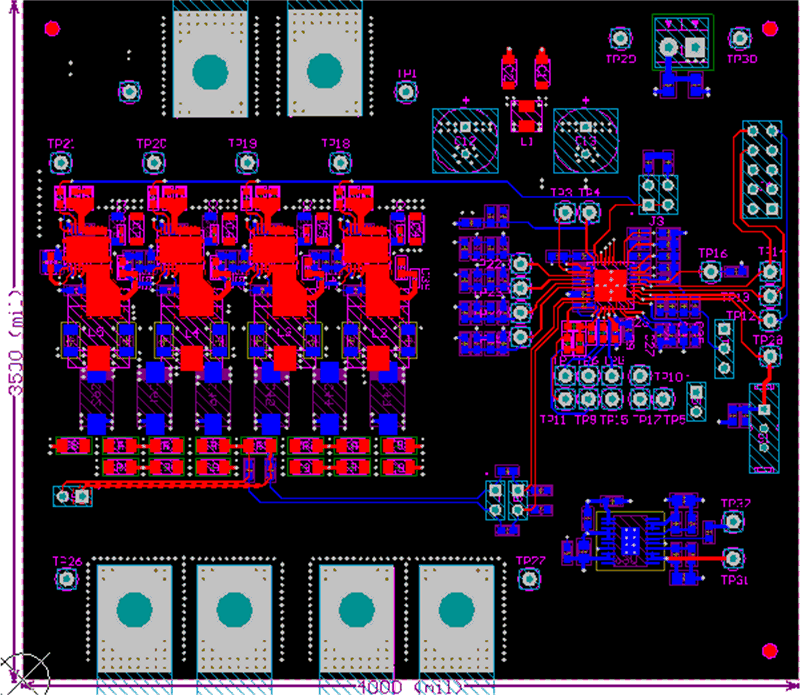 Figure 124. TPS53647 Layout Example