SLUSB56B November 2012 – April 2019 TPS53819A
PRODUCTION DATA.
- 1 Features
- 2 Applications
- 3 Description
- 4 Revision History
- 5 Pin Configuration and Functions
- 6 Specifications
-
7 Detailed Description
- 7.1 Overview
- 7.2 Functional Block Diagram
- 7.3
Feature Description
- 7.3.1 Enable and Soft-Start
- 7.3.2 Adaptive On-Time Control
- 7.3.3 Zero Crossing Detection
- 7.3.4 Output Discharge Control
- 7.3.5 Low-Side Driver
- 7.3.6 High-Side Driver
- 7.3.7 Power Good
- 7.3.8 Current Sense and Overcurrent Protection
- 7.3.9 Overvoltage and Undervoltage Protection
- 7.3.10 Out-of-Bound Protection
- 7.3.11 UVLO Protection
- 7.3.12 Thermal Shutdown
- 7.4 Device Functional Modes
- 7.5 Programming
- 7.6
Register Maps
- 7.6.1 OPERATION [01h] (R/W Byte)
- 7.6.2 ON_OFF_CONFIG [02h] (R/W Byte)
- 7.6.3 WRITE_PROTECT [10h] (R/W Byte)
- 7.6.4 CLEAR_FAULTS [03h] (Send Byte)
- 7.6.5 STORE_DEFAULT_ALL [11h] (Send Byte)
- 7.6.6 RESTORE_DEFAULT_ALL [12h] (Send Byte)
- 7.6.7 STATUS_WORD [79h] (Read Word)
- 7.6.8 CUSTOM_REG (MFR_SPECIFIC_00) [D0h] (R/W Byte)
- 7.6.9 DELAY_CONTROL (MFR_SPECIFIC_01) [D1h] (R/W Byte)
- 7.6.10 MODE_SOFT_START_CONFIG (MFR_SPECIFIC_02) [D2h] (R/W Byte)
- 7.6.11 FREQUENCY_CONFIG (MFR_SPECIFIC_03) [D3h] (R/W Byte)
- 7.6.12 VOUT_ADJUSTMENT (MFR_SPECIFIC_04) [D4h] (R/W Byte)
- 7.6.13 Output Voltage Fine Adjustment Soft Slew Rate
- 7.6.14 VOUT_MARGIN (MFR_SPECIFIC_05) [D5h] (R/W Byte)
- 7.6.15 Output Voltage Margin Adjustment Soft-Slew Rate
- 7.6.16 UVLO_THRESHOLD (MFR_SPECIFIC_06) [D6h]
-
8 Application and Implementation
- 8.1 Application Information
- 8.2
Typical Application
- 8.2.1 Design Requirements
- 8.2.2
Detailed Design Procedure
- 8.2.2.1 Custom Design With WEBENCH® Tools
- 8.2.2.2 Switching Frequency
- 8.2.2.3 Inductor (L1)
- 8.2.2.4 Output Capacitors (C10, C11, C12, C13, C14)
- 8.2.2.5 Input Capacitors (C1, C2, C3, C4, C5)
- 8.2.2.6 MOSFET (Q1, Q2)
- 8.2.2.7 VREG Bypass Capacitor (C18)
- 8.2.2.8 VDD Bypass Capacitor (C19)
- 8.2.2.9 VBST Capacitor (C7)
- 8.2.2.10 Snubber (C8 and R9)
- 8.2.2.11 Feedback Resistance, RFBH and RFBL (R17 and R18)
- 8.2.2.12 Overcurrent Limit (OCL) Setting Resistance (R10)
- 8.2.2.13 PMBus Device Address (R3 and R4)
- 8.2.2.14 PGOOD Pullup Resistor (R2)
- 8.2.2.15 SCL and SDA Pulldown Resistors (R14 and R15)
- 8.2.2.16 PMBus Pullup Resistors
- 8.2.3 Application Curves
- 9 Power Supply Recommendations
- 10Layout
- 11Device and Documentation Support
- 12Mechanical, Packaging, and Orderable Information
Package Options
Mechanical Data (Package|Pins)
- RGT|16
Thermal pad, mechanical data (Package|Pins)
- RGT|16
Orderable Information
6.8 Typical Characteristics
 Figure 1. VDD Supply Current vs Temperature
  Figure 3. OVP/UVP Thresholds vs Temperature
  Figure 5. No-Load Start-Up Waveforms with DCM
  Figure 7. Full-Load Start-Up Waveforms
  Figure 9. Pre-Bias Start-Up Waveforms with FCCM
  Figure 11. No-Load Shutdown Waveforms with FCCM
  Figure 13. No-Load UVLO Start-Up Waveforms
  Figure 15. 1.2-V Output Ripple with FCCM
  Figure 17. CCM to DCM Transitions
  Figure 19. FCCM Load Transients
  Figure 21. Output Short Circuit Protection with Hiccup
  Figure 23. No-Load VOUT Adjustment Waveforms


 Figure 2. VDD Shutdown Current vs Temperature
  Figure 4. TRIP Pin Current vs Temperature
  Figure 6. No-Load Start-Up Waveforms with FCCM
  Figure 8. Pre-Bias Start-Up Waveforms with DCM
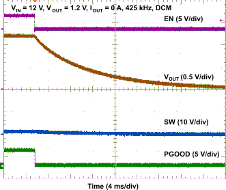
  Figure 10. No-Load Shutdown Waveforms with DCM
  Figure 12. Full-Load Shutdown Waveforms
  Figure 14. Full-Load UVLO Start-Up Waveforms
  Figure 16. 1.2-V Output Ripple with DCM
  Figure 18. DCM to CCM Transitions
  Figure 20. DCM Load Transients
  Figure 22. Output Short Circuit Protection with Latch-off
  Figure 24. Full-Load VOUT Adjustment Waveforms


