SLUSAS9B NOVEMBER 2013 – December 2014 TPS53915
PRODUCTION DATA.
- 1 Features
- 2 Applications
- 3 Description
- 4 Revision History
- 5 Pin Configuration and Functions
- 6 Specifications
-
7 Detailed Description
- 7.1 Overview
- 7.2 Functional Block Diagrams
- 7.3
Feature Description
- 7.3.1 Powergood
- 7.3.2 D-CAP3 Control and Mode Selection
- 7.3.3 D-CAP3 Mode
- 7.3.4 Sample and Hold Circuitry
- 7.3.5 Adaptive Zero-Crossing
- 7.3.6 Forced Continuous-Conduction Mode
- 7.3.7 Current Sense and Overcurrent Protection
- 7.3.8 Overvoltage and Undervoltage Protection
- 7.3.9 Out-Of-Bounds Operation (OOB)
- 7.3.10 UVLO Protection
- 7.3.11 Thermal Shutdown
- 7.4 Device Functional Modes
- 7.5
Programming
- 7.5.1 The PMBus General Descriptions
- 7.5.2 PMBus Slave Address Selection
- 7.5.3 PMBus Address Selection
- 7.5.4 Supported Formats
- 7.5.5 Supported PMBus Commands
- 7.5.6 CLEAR_FAULTS [03h] (Send Byte)
- 7.5.7 STORE_DEFAULT_ALL [11h] (Send Byte)
- 7.5.8 RESTORE_DEFAULT_ALL [12h] (Send Byte)
- 7.5.9 STATUS_WORD [79h] (Read Word)
- 7.5.10 CUSTOM_REG (MFR_SPECIFIC_00) [D0h] (R/W Byte)
- 7.5.11 DELAY_CONTROL (MFR_SPECIFIC_01) [D1h] (R/W Byte)
- 7.5.12 MODE_SOFT_START_CONFIG (MFR_SPECIFIC_02) [D2h] (R/W Byte)
- 7.5.13 FREQUENCY_CONFIG (MFR_SPECIFIC_03) [D3h] (R/W Byte)
- 7.5.14 VOUT_ADJUSTMENT (MFR_SPECIFIC_04) [D4h] (R/W Byte)
- 7.5.15 Output Voltage Fine Adjustment Soft Slew Rate
- 7.5.16 VOUT_MARGIN (MFR_SPECIFIC_05) [D5h] (R/W Byte)
- 7.5.17 Output Voltage Margin Adjustment Soft-Slew Rate
- 7.5.18 UVLO_THRESHOLD (MFR_SPECIFIC_06) [D6h]
- 8 Application and Implementation
- 9 Power Supply Recommendations
- 10Layout
- 11Device and Documentation Support
- 12Mechanical, Packaging, and Orderable Information
Package Options
Mechanical Data (Package|Pins)
- RVE|28
Thermal pad, mechanical data (Package|Pins)
- RVE|28
Orderable Information
1 Features
- Integrated 13.8– and 5.9-mΩ MOSFETs Support 12-A Continuous Output Current
- Adjustments Available Through PMBus™
- Voltage Margin and Adjustment
- Soft-Start Time
- Power-On Delay
- VDD UVLO Level
- Fault Reporting
- Switching Frequency
- Supports All Ceramic Output Capacitors
- Reference Voltage 600 mV ±0.5% Tolerance
- Output Voltage Range: 0.6 V to 5.5 V
- D-CAP3™ Control Mode With Fast Load-Step Response
- Auto-Skipping Eco-Mode™ for High Light-Load Efficiency
- FCCM for Tight Output Ripple and Voltage Requirements
- Eight Selectable Frequency Settings from
200 kHz to 1 MHz - 3.5 mm × 4.5 mm, 28-Pin, QFN Package
2 Applications
- Server and Cloud-Computing Point-of-Load (POL) Products
- Broadband, Networking, and Optical Communications Infrastructure
- I/O Supplies
- Supported at the WEBENCH™ Design Center
3 Description
The TPS53915 is a small-sized, synchronous buck converter with an adaptive on-time D-CAP3 control mode. The device offers ease-of-use and low external-component count for space-conscious power systems.
This device features high-performance integrated MOSFETs, accurate 0.5% 0.6-V reference, and an integrated boost switch. Competitive features include very-low external-component count, fast load-transient response, auto-skip mode operation, internal soft-start control, and no requirement for compensation. The device also features programmability and fault report via PMBus™ to simplify the power supply design.
A forced continuous conduction mode helps meet tight voltage regulation accuracy requirements for performance DSPs and FPGAs. The TPS53915 is available in a 28-pin QFN package and is specified from –40°C to 85°C ambient temperature.
Device Information(1)
| PART NUMBER | PACKAGE | BODY SIZE (NOM) |
|---|---|---|
| TPS53915 | VQFN-CLIP (28) | 4.50 mm x 3.50 mm |
- For all available packages, see the orderable addendum at the end of the datasheet.
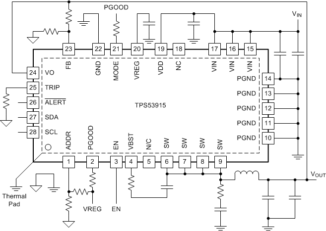
Simplified Schematic

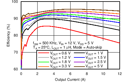
Efficiency vs Output Current
