SLVSA23A September 2009 – January 2024 TPS5410-Q1
PRODUCTION DATA
- 1
- 1Features
- 2Applications
- 3Description
- 4Electrostatic Discharge Caution
- 5Ordering Information
- 6Pin Assignments
- 7Specifications
-
8Application Information
- 8.1 Functional Block Diagram
- 8.2
Detailed Description
- 8.2.1 Oscillator Frequency
- 8.2.2 Voltage Reference
- 8.2.3 Enable (ENA) and Internal Slow Start
- 8.2.4 Undervoltage Lockout (UVLO)
- 8.2.5 Boost Capacitor (BOOT)
- 8.2.6 Output Feedback (VSENSE)
- 8.2.7 Internal Compensation
- 8.2.8 Voltage Feed Forward
- 8.2.9 Pulse-Width-Modulation (PWM) Control
- 8.2.10 Overcurrent Liming
- 8.2.11 Overvoltage Protection
- 8.2.12 Thermal Shutdown
- 8.2.13 PCB Layout
- 8.2.14 Application Circuits
- 8.2.15 Design Procedure
- 8.2.16 Output Filter Capacitor Selection
- 8.2.17 External Compensation Network
- 8.3 Advanced Information
- 8.4 Performance Graphs
- 8.5 Performance Graphs
- 9Revision History
Package Options
Mechanical Data (Package|Pins)
- D|8
Thermal pad, mechanical data (Package|Pins)
Orderable Information
8.2.13 PCB Layout
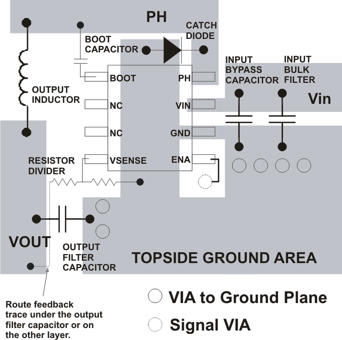
Connect a low ESR ceramic bypass capacitor to the VIN pin. Care should be taken to minimize the loop area formed by the bypass capacitor connections, the VIN pin, and the TPS5410 ground pin. The best way to do this is to extend the top side ground area from under the device adjacent to the VIN trace, and place the bypass capacitor as close as possible to the VIN pin. The minimum recommended bypass capacitance is 4.7μF ceramic with a X5R or X7R dielectric.
There should be a ground area on the top layer directly underneath the IC to connect the GND pin of the device and the anode of the catch diode. The GND pin should be tied to the PCB ground by connecting it to the ground area under the device as shown in Figure 8-1.
The PH pin should be routed to the output inductor, catch diode and boot capacitor. Since the PH connection is the switching node, the inductor should be located close to the PH pin, and the area of the PCB conductor minimized to prevent excessive capacitive coupling. The catch diode should also be placed close to the device to minimize the output current loop area. Connect the boot capacitor between the phase node and the BOOT pin as shown. Keep the boot capacitor close to the IC and minimize the conductor trace lengths. The component placements and connections shown work well, but other connection routings may also be effective.
Connect the output filter capacitor(s) as shown between the VOUT trace and GND. It is important to keep the loop formed by the PH pin, Lout, Cout and GND as small as is practical.
Connect the VOUT trace to the VSENSE pin using the resistor divider network to set the output voltage. Do not route this trace too close to the PH trace. Due to the size of the IC package and the device pinout, the trace may need to be routed under the output capacitor. The routing may be done on an alternate layer if a trace under the output capacitor is not desired.
If the grounding scheme shown is used via a connection to a different layer to route to the ENA pin.
 Figure 8-1 Design Layout
 Figure 8-2 TPS5410 Land Pattern