SLVS675E August   2006  – January 2024 TPS5410

PRODUCTION DATA  

  1.   1
  2. Features
  3. Applications
  4. Description
  5. Pin Configuration and Functions
  6. Specifications
    1. 5.1 Absolute Maximum Ratings
    2. 5.2 ESD Ratings
    3. 5.3 Recommended Operating Conditions
    4. 5.4 Thermal Information 
    5. 5.5 Electrical Characteristics
    6. 5.6 Typical Characteristics
  7. Detailed Description
    1. 6.1 Overview
    2. 6.2 Functional Block Diagram
    3. 6.3 Feature Description
      1. 6.3.1  Oscillator Frequency
      2. 6.3.2  Voltage Reference
      3. 6.3.3  Enable (ENA) and Internal Slow-Start
      4. 6.3.4  Undervoltage Lockout (UVLO)
      5. 6.3.5  Boost Capacitor (BOOT)
      6. 6.3.6  Output Feedback (VSENSE)
      7. 6.3.7  Internal Compensation
      8. 6.3.8  Voltage Feed-Forward
      9. 6.3.9  Pulse-Width-Modulation (PWM) Control
      10. 6.3.10 Overcurrent Limiting
      11. 6.3.11 Overvoltage Protection
      12. 6.3.12 Thermal Shutdown
    4. 6.4 Device Functional Modes
      1. 6.4.1 Minimum Input Voltage
      2. 6.4.2 ENA Control
  8. Applications and Implementation
    1. 7.1 Application Information
    2. 7.2 Typical Applications
      1. 7.2.1 Application Circuit
        1. 7.2.1.1 Design Requirements
        2. 7.2.1.2 Detailed Design Procedure
          1. 7.2.1.2.1 Switching Frequency
          2. 7.2.1.2.2 Input Capacitors
          3. 7.2.1.2.3 Output Filter Components
            1. 7.2.1.2.3.1 Inductor Selection
            2. 7.2.1.2.3.2 Capacitor Selection
          4. 7.2.1.2.4 Output Voltage Setpoint
          5. 7.2.1.2.5 Boot Capacitor
          6. 7.2.1.2.6 Catch Diode
          7. 7.2.1.2.7 Advanced Information
            1. 7.2.1.2.7.1 Output Voltage Limitations
            2. 7.2.1.2.7.2 Internal Compensation Network
            3. 7.2.1.2.7.3 Thermal Calculations
        3. 7.2.1.3 Application Curves
      2. 7.2.2 Using All Ceramic Capacitors
        1. 7.2.2.1 Design Requirements
        2. 7.2.2.2 Detailed Design Procedure
          1. 7.2.2.2.1 Output Filter Capacitor Selection
          2. 7.2.2.2.2 External Compensation Network
        3. 7.2.2.3 Application Curves
    3. 7.3 Power Supply Recommendations
    4. 7.4 Layout
      1. 7.4.1 Layout Guidelines
      2. 7.4.2 Layout Example
  9. Device and Documentation Support
    1. 8.1 Documentation Support
      1. 8.1.1 Related Documentation
    2. 8.2 Receiving Notification of Documentation Updates
    3. 8.3 Support Resources
    4. 8.4 Trademarks
    5. 8.5 Electrostatic Discharge Caution
    6. 8.6 Glossary
  10. Revision History
  11. 10Mechanical, Packaging, and Orderable Information

Package Options

Mechanical Data (Package|Pins)
Thermal pad, mechanical data (Package|Pins)
Orderable Information

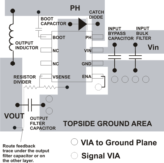
Layout Example

GUID-0BE704EA-A0C8-4A67-AD34-23309BEA6BF4-low.gifFigure 7-17 Design Layout
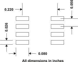
GUID-2A749AA7-F053-4D91-99F3-BB657CAA0ADC-low.gifFigure 7-18 TPS5410 Land Pattern