TPS54140 1.5-A, 42-V Step-Down DC-DC Converter With Eco-mode™
1 Features
- 3.5- to 42-V Input Voltage Range
- 200-mΩ High-Side MOSFET
- High Efficiency at Light Loads with a Pulse Skipping Eco-mode™
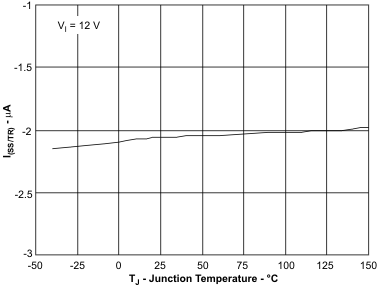
- 116-μA Operating Quiescent Current
- 1.3-μA Shutdown Current
- 100-kHz to 2.5-MHz Switching Frequency
- Synchronizes to External Clock
- Adjustable Slow Start and Sequencing
- UV and OV Power-Good Output
- Adjustable UVLO Voltage and Hysteresis
- 0.8-V Internal Voltage Reference
- MSOP10 Package With PowerPAD™
- Supported by WEBENCH® Software Tool (www.TI.com/WEBENCH)
2 Applications
- 12-V and 24-V Industrial and Commercial Low Power Systems
- Aftermarket Auto Accessories: Video, GPS, Entertainment
3 Description
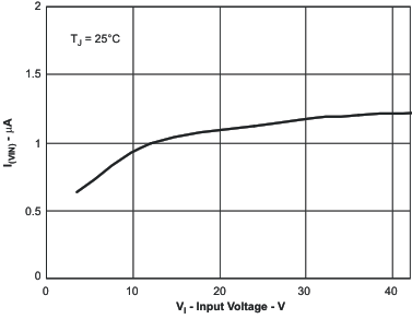
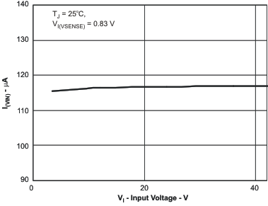
The TPS54140 device is a 42-V, 1.5-A, step-down regulator with an integrated high-side MOSFET. Current mode control provides simple external compensation and flexible component selection. A low-ripple pulse-skip mode reduces the no load, regulated output-supply current to 116 μA. Using the enable pin, the shutdown supply current is reduced to 1.3 μA.
Undervoltage lockout is internally set at 2.5 V, but can be increased using the enable pin. The output-voltage startup ramp is controlled by the slow-start pin that can also be configured for sequencing and tracking. An open-drain power-good signal indicates the output is within 94% to 107% of the nominal voltage.
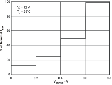
A wide switching frequency range allows efficiency and external component size to be optimized. Frequency foldback and thermal shutdown protects the device during an overload condition.
The TPS54140 device is available in a 10-pin thermally enhanced MSOP PowerPAD package.
Device Information(1)
| PART NUMBER | PACKAGE | BODY SIZE (NOM) |
|---|---|---|
| TPS54140 | MSOP (10) | 3.00 mm × 3.00 mm |
- For all available packages, see the orderable addendum at the end of the datasheet.
4 Simplified Schematic

Efficiency vs Load Current

5 Revision History
Changes from B Revision (September 2013) to C Revision
- Added the Handling Ratings table and the following sections:Feature Description, Device Functional Modes, Application and Implementation, Power Supply Recommendations, Device and Documentation Support, and Mechanical, Packaging, and Orderable InformationGo
Changes from A Revision (August 2012) to B Revision
- Deleted SWIFT from the data sheet Title and FeaturesGo
Changes from * Revision (October 2008) to A Revision
- Changed Features Item From: 300kHz to 2.5MHz Switching Frequency To: 100kHz to 2.5MHz Switching FrequencyGo
- Changed Description text From: "within 93% to 107% of its nom voltage." To: "within 94% to 107% of its nom voltage."Go
- Changed Enable threshold +50 mV TYP value From: ±3.8 To: –3.8Go
- Changed Enable threshold ±50 mV TYP value From: ±0.9 To: –0.98Go
- Changed Hysteresis current TYP value From: ±2.9 To: –2.9Go
- Changed Error amplifier transconductance (gM) Test Condition From: ±2 μA < ICOMP < 2 μA, VCOMP = 1 V To: –2 μA < ICOMP < 2 μA, VCOMP = 1 VGo
- Changed Error amplifier transconductance (gM) during slow start From: ±2 μA < ICOMP < 2 μA, VCOMP = 1 V To: –2 μA < ICOMP < 2 μA, VCOMP = 1 VGo
- Changed text in the Error Amplifier section From: "the gm is 25 μA/V" To: "the gm is 26 μA/V" Go
- Changed text in the Slow Start and Tracking Pin (SS/TR) section From: "VIN UVLO is exceeded, EN pin pulled below 1.25V" To: "VIN pin is below the VIN UVLO, EN pin pulled below 1.25V"Go
- Changed Start Input Voltage (rising VIN) voltage From: 7.25 V To: 7.7 VGo
- Changed Start Input Voltage (falling VIN) voltage From: 6.25 V To: 6.7 VGo
- Changed Equation 29Go
- Changed 7.25V to 7.7V and 6.25V to 6.7V in the Under Voltage Lock Out Set Point section.Go
- Changed Equation 47Go
- Changed Equation 49Go
6 Pin Configuration and Functions

Pin Functions
| PIN | I/O | DESCRIPTION | ||
|---|---|---|---|---|
| NO. | NAME | |||
| 1 | BOOT | O | A bootstrap capacitor is required between the BOOT and PH pins. If the voltage on this capacitor is below the minimum required by the device, the output is forced to switch off until the capacitor is refreshed. | |
| 2 | VIN | I | This pin is the 3.5- to 42-V input supply voltage. | |
| 3 | EN | I | This pin is the enable pin and internal pullup current source. To disable, pull below 1.2 V. Float this pin to enable. Adjust the input undervoltage lockout with two resistors. | |
| 4 | SS/TR | I | This pin is the slow-start and tracking pin. An external capacitor connected to this pin sets the output rise time. Because the voltage on this pin overrides the internal reference, it can be used for tracking and sequencing. | |
| 5 | RT/CLK | I | This pin is the resistor timing and external clock pin. An internal amplifier holds this pin at a fixed voltage when using an external resistor to ground to set the switching frequency. If the pin is pulled above the PLL upper threshold, a mode change occurs and the pin becomes a synchronization input. The internal amplifier is disabled and the pin is a high impedance clock input to the internal PLL. If clocking edges stop, the internal amplifier is re-enabled and the mode returns to a resistor set function. | |
| 6 | PWRGD | O | This pin is an open drain output. This pin is asserted low if the output voltage is low because of thermal shutdown, dropout, overvoltage, or EN shut down. | |
| 7 | VSENSE | I | This pin is the inverting node of the transconductance (gm) error amplifier. | |
| 8 | COMP | O | This pin is the error amplifier output and input to the output-switch current comparator. Connect frequency compensation components to this pin. | |
| 9 | GND | — | Ground pin | |
| 10 | PH | O | This pin is the source of the internal high-side power MOSFET. | |
| 11 | Thermal Pad | — | The GND pin must be electrically connected to the exposed pad on the printed circuit board for proper operation. | |
7 Specifications
7.1 Absolute Maximum Ratings(1)
Over operating temperature range (unless otherwise noted).| MIN | MAX | UNIT | ||
|---|---|---|---|---|
| Input voltage | VIN | –0.3 | 47 | V |
| EN | –0.3 | 5 | ||
| BOOT | 55 | |||
| VSENSE | –0.3 | 3 | ||
| COMP | –0.3 | 3 | ||
| PWRGD | –0.3 | 6 | ||
| SS/TR | –0.3 | 3 | ||
| RT/CLK | –0.3 | 3.6 | ||
| Output voltage | PH–BOOT | 8 | V | |
| PH | –0.6 | 47 | ||
| PH, 10-ns Transient | –2 | 47 | ||
| Voltage Difference | PAD to GND | ±200 | mV | |
| Source current | EN | 100 | μA | |
| BOOT | 100 | mA | ||
| VSENSE | 10 | μA | ||
| PH | Current Limit | A | ||
| RT/CLK | 100 | μA | ||
| Sink current | VIN | Current Limit | A | |
| COMP | 100 | μA | ||
| PWRGD | 10 | mA | ||
| SS/TR | 200 | μA | ||
| Operating junction temperature | –40 | 150 | °C | |
7.2 Handling Ratings
| MIN | MAX | UNIT | |||
|---|---|---|---|---|---|
| Tstg | Storage temperature range | –65 | 150 | °C | |
| V(ESD) | Electrostatic discharge | Human body model (HBM), per ANSI/ESDA/JEDEC JS-001, all pins(1) | –1 | 1 | kV |
| Charged device model (CDM), per JEDEC specification JESD22-C101, all pins(2) | –500 | 500 | V | ||
7.3 Recommended Operating Conditions
Over operating free-air temperature range (unless otherwise noted)| MIN | NOM | MAX | UNIT | ||
|---|---|---|---|---|---|
| Operating input voltage on the VIN pin | 3.5 | 42 | V | ||
| Output voltage | 0.8 | 39 | V | ||
| Output current | 0 | 1.5 | A | ||
| TJ | Operating junction temperature | –40 | 150 | °C | |
7.4 Thermal Information
| THERMAL METRIC(1) | DGQ | UNIT | |
|---|---|---|---|
| 10 PINS | |||
| RθJA | Junction-to-ambient thermal resistance | 67.4 | °C/W |
| RθJC(top) | Junction-to-case (top) thermal resistance | 46.7 | |
| RθJB | Junction-to-board thermal resistance | 38.4 | |
| ψJT | Junction-to-top characterization parameter | 1.9 | |
| ψJB | Junction-to-board characterization parameter | 38.4 | |
| RθJC(bot) | Junction-to-case (bottom) thermal resistance | 46.7 | |
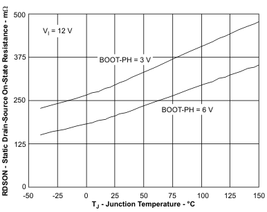
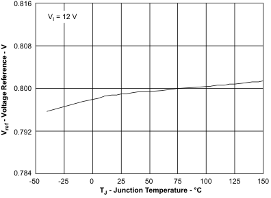
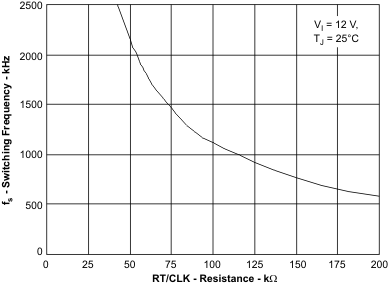
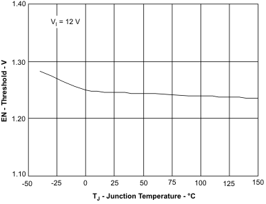
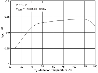
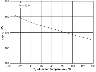
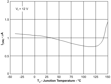
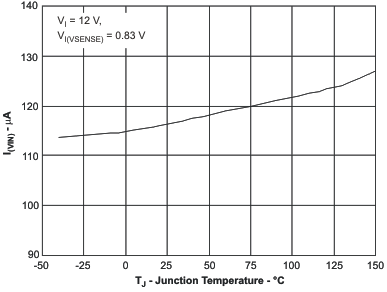
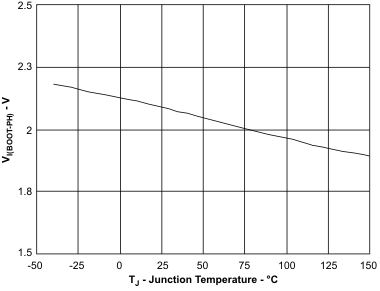
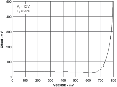
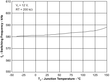
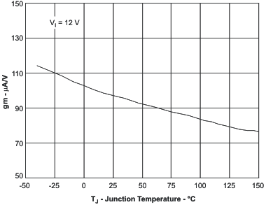
7.5 Electrical Characteristics
TJ = –40°C to 150°C, VIN = 3.5 to 42V (unless otherwise noted)7.6 Typical Characteristics